Microsemi Licenses Crossbar ReRAM Non-Volatile Memory
by Billy Tallis on May 16, 2018 8:00 AM EST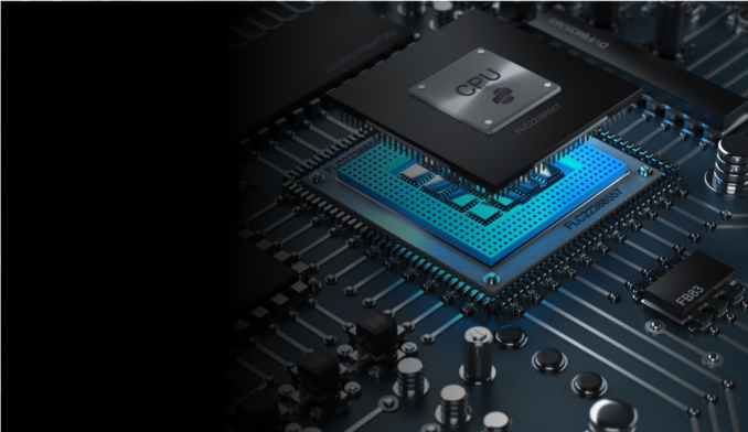
Crossbar, Inc. has announced Microsemi as the first licensee for their embedded Resistive RAM (ReRAM) memory technology. ReRAM is one of several up and coming non-volatile memory technologies, and is one of the more promising potential competitors to Intel's 3D XPoint memory. Crossbar has been developing their flavor of ReRAM for years and currently fabricates the memory on a 40nm process at SMIC. They now have a new fab partner that can manufacture ReRAM on a 1x nm process, and it is this capability that has attracted their first major customer. Microsemi has a very broad product catalog, and they aren't ready to reveal what they plan to use ReRAM for. The embedded ReRAM technology from Crossbar will enable Microsemi to add blocks of ReRAM to the ASICs they are designing for production on an advanced 1x nm process.
Crossbar touts compatibility with standard CMOS fabrication processes as one of the key advantages of their ReRAM over new non-volatile memory technologies. Manufacturing ReRAM only requires adding a few extra steps to the back end of line wafer processing, and doesn't require radical changes to the materials involved. Crossbar now has plans for commercial production of ReRAM on a 1x nm node and they claim that it can scale down to processes smaller than 10nm. This is expected to make Crossbar's ReRAM a relatively inexpensive embedded memory that won't impose serious constraints on the rest of the ASIC. By contrast, Everspin's magnetoresistive RAM (MRAM)—which is also currently being manufactured on a 40nm process—will be moving to GlobalFoundries 22nm FD-SOI this year but probably won't be available on a high-performance FinFET process in the near future. Embedded flash memory has trouble scaling below about 40nm while retaining the endurance typically required of embedded memories, and 3D NAND cannot be easily added to a logic process.
Like most new non-volatile memory technologies, ReRAM isn't ready to compete head-on against DRAM or NAND flash memory. Its first path to commercialization is therefore through use as a special-purpose embedded memory, where its different tradeoffs between performance, endurance and density make it a good fit for certain applications. Currently, Crossbar quotes performance as read latencies on the order of 10ns, write latencies around 10µs, and write endurance in excess of 1M cycles. ReRAM is also accessible at the byte level instead of using large erase blocks like flash memory. Crossbar expects 10 years of data retention and has not observed problems with read or write operations disturbing the state of adjacent memory cells.
Separately from the new Microsemi partnership, Crossbar will also soon be demonstrating the use of their embedded ReRAM in an in-memory compute architecture for AI. At the Embedded Vision Summit next week, Crossbar will demonstrate object and facial recognition based on a pre-trained FaceNet model stored in ReRAM. Since the memory is on the same chip as the compute elements of the neural network, it can use very wide data paths to offer high performance without the high power draw that an external DRAM solution like HBM would bring or the much larger die area that SRAM would require. Facial recognition is an appropriately read-heavy workload for ReRAM, but the ReRAM will have no trouble handling the model updates that result from registering new faces. The demo is intended to show how ReRAM can be useful for AI tasks on battery-powered devices that don't have the option of offloading their computational workload to the cloud. Because ReRAM is non-volatile, the AI chip can be powered down but is instantly ready to perform recognition upon waking up, without having to re-load the model from storage into SRAM or DRAM. Since this demo chip is still using a 40nm manufacturing process and is just intended as a proof of concept, the embedded ReRAM array is only a single megabyte, but Crossbar expects that similar chips made on the 1x nm process that will soon be available would use many MB of ReRAM to support more complex models while still offering extremely high and consistent recognition performance.


9 Comments
View All Comments
plopke - Wednesday, May 16, 2018 - link
Aaah this article reminds me of HP memristor , "100TB drives by 2018" , "it will replace Flash and in some cases RAM". So far the only one coming close is Intel/Micron but a few years of delay , well lets hope these guys make it and are not held back by patents or lack of mass production to bring it to market!ImSpartacus - Wednesday, May 16, 2018 - link
Yeah, we've been burnt so many times by overzealous claims that I've become rather pessimistic about new memory tech.Obviously I hope for the best, but I'm not holding my breath.
mode_13h - Friday, May 18, 2018 - link
Burnt? You had some financial stake in any of these promises?No need to get "burnt" this time - they aren't even claiming the same performance levels as 3D XPoint, so keep your expectations in check. Write latencies around 10 microseconds puts this more on par with NVMe flash.
Santoval - Monday, May 21, 2018 - link
True, write latencies are comparable to flash but read latencies are 1000 times faster, about as fast as L2 cache. So ReRAM could be employed in read-intensive workloads (in place of the pitifully slow QLC flash, which also has a pathetic endurance) - if they manage a high enough density. ReRAM's performance is highly .. asymmetric, but if you can have the write speed of flash with the read speed of L2 cache it is not a bad deal at all.wumpus - Friday, May 18, 2018 - link
You're reading the wrong things into this. As stated, ReRam can't compete with either Flash or DRAM for storage, so they really aren't trying to sell to *you*. They are selling it to ASIC designers who don't want to pay for an extra chip on the board, nor the extra pins and connections.Putting memory on a chip is a pain. For small sizes, just slap down 6 transistors for a SRAM bit and go. You can pretty much expect to find this anywhere you need to scatter storage in the chip, and famously in the caches of CPUs.
I'm guessing that they can access ReRAM far easier than Flash (which has to be read in fairly large batches and written [well erased] in huge batches). DRAM on a chip is also problematic, in that the transistors themselves don't really match the logic processes that ASICs use (check the sizes sometime: embedded DRAM transistors are something like 10 times as big, and use a vastly smaller process). DRAM has enough overhead (all the sensors and such, but I suspect that ReRAM is at least as bad) that when combined with the extra-large transistors you tend to only cram twice the memory in the same [large] area as SRAM. Presumably ReRAM beats this.
But comparing embedded ReRAM to DRAM made on a DRAM chip or large amounts of FLASH? Won't happen and this article says as much. You won't see it in your computer (soon), you won't see it in your phone, you *might* see it in the embedded processor in your toaster.
Still, if they can ship a product they can keep the labs running. And who knows what type of advantages it might have at 0xnm.
Dragonstongue - Wednesday, May 16, 2018 - link
cheers to this...maybe this will allow lower cost higher performance memory for SSD, RAM or whatever they can envision, we NEED competition in the tech industry to keep prices "honest" afterall ^.^mode_13h - Friday, May 18, 2018 - link
Go back and re-read the article!This is neither about density nor $ per GB! It's about low read latency, high endurance (relative to NAND), and long retention.
MrSpadge - Wednesday, May 16, 2018 - link
Yeah, HP was very bold with its claims back then. And there's good reason to be sceptic about any new memory technology. They may be excel in 2 or 3 attributes, but lack in another important one. That's enough to keep them from taking over the market or even entering it. However, I would say Crossbar is above average in this regard. Several factors are aligning favorably, so they may actually succed in some ways.BubbaJones - Monday, April 15, 2019 - link
Pretty crazy being approached recently by old friends (architects) in the PCM biz, asking if I had ideas how to better use a bunch of 3DXPoint managed behind a NVMe front end. Well, when your low-level PCM device interface is ill-conceived it's really hard not to aggregate as anything but a block device. Like storage protocols before NVMe, we already figured out how to hide latency. 3DXPoint doesn't buy you that much. Should have listened...now back to the drawing board boys.