Samsung's Next-Gen 3nm and 4nm Nodes on Track for Mass Production in 2H 2024
by Anton Shilov on November 2, 2023 7:00 PM EST- Posted in
- Semiconductors
- Samsung Foundry
- 3nm
- 4nm
- SF3
- SF4X
Samsung is set to start making chips using its 2nd Generation 3nm-class (SF3) manufacturing technology as well as performance-enhanced version of its 4nm-class (SF4X) fabrication process in the second half of next year, the company told its investors this week. Both production nodes are expected to significantly improve competitive positions of the company as they will enable it to build new types of products.
"We will strengthen our technology competitiveness through the 2H [2024] mass production of the 2nd generation 3nm process as well as the 4th generation 4nm process for HPC," a statement by the company reads. "The market is forecast to shift to growth thanks to a rebound in mobile demand and continued growth in HPC demand."
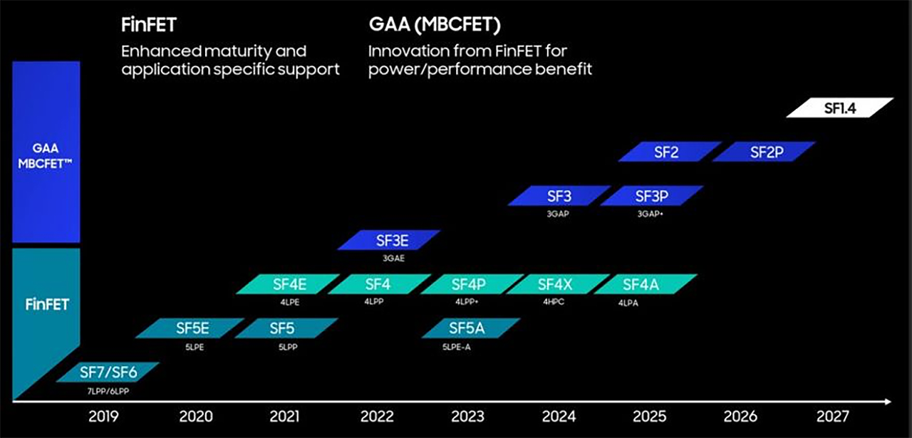
Samsung's forthcoming SF3 process technology is a major upgrade to its existing SF3E production node, which, based on the available knowledge, is only used to make small chips for cryptocurrency mining. Samsung asserts that the SF3 will offer greater design versatility by allowing for different gate-all-around (GAA) transistor's nanosheet channel widths within the same cell type.
Although Samsung does not make direct comparisons between SF3 and SF3E, it says that SF3 offers major improvements over SF4 (4LPP, 4nm-class, low power plus), which includes a 22% increase in performance at equivalent power and complexity, or alternatively, a 34% reduction in power consumption at the same frequency and transistor count, along with a 21% reduction in logic area. In general, it is expected that SF3 will be a better option for complex designs than SF3E, though it will enter high-volume production in the second half of 2024.
In the meantime, Samsung Foundry's 4nm-class generation nodes continue to evolve. The company gearing up to launch its SF4X (4HPC, 4 nm-class high-performance computing) process technology, tailored for high-performance applications such as CPUs and GPUs used in data centers. This one is going to be SF's first process node in recent years that has been specifically designed for high-performance computing (HPC) applications.
Samsung's SF4X process technology promises to deliver a 10% improvement in performance along with a 23% reduction in power consumption. While Samsung has not disclosed the baseline for this comparison, it is likely in reference to their standard SF4 (4LPP) process. This enhancement is achieved through a redesign of the transistor's source and drain regions, following a reassessment of their performance under potentially high-stress conditions, the application of advanced transistor-level design-technology co-optimization (T-DTCO), and the implementation of a new middle-of-line (MOL) architecture.
With refined MOL architecture, SF4X is expected to achieve a silicon-validated minimum operating voltage (Vmin) for CPUs at 60mV, reduce the variability in the off-state current (IDDQ) by 10%, ensure stable high voltage (Vdd) operation above 1V without compromising performance, and enhance process margin for SRAM.
Source: Samsung


9 Comments
View All Comments
Dante Verizon - Friday, November 3, 2023 - link
Fingers crossed for them.NextGen_Gamer - Friday, November 3, 2023 - link
Honestly, yes, fingers crossed. Same for Intel's foundry business. TSMC has been rocking it, for sure, but because they have been consistently delivering great nodes with great yields, they also know they can charge a fortune for them. To have some real competition in the area would force TSMC to be competitive on wafer prices as well, which directly leads to lower prices for consumers.Dante Verizon - Friday, November 3, 2023 - link
One question is if it's so hard to shrink caches, why don't they use 3D stacking like in nand and HBM?SiliconJock - Friday, November 3, 2023 - link
Well, cache is SRAM whereas NAND and HBM are flash memory and DRAM, respectively.Two (three) different animals.
Anyhow, AMD's X3D CPUs have stacked SRAM but it's not all that easy to implement - nor is it reliable, if 5800X3D's various problems are any indicator.
Dante Verizon - Friday, November 3, 2023 - link
The lower clock rate is a small issue compared to the gain in performance and success of the x3D models. Anyway, the X3D is two different dies connected to each other later.I thought about doing the stacking directly in the design process on a single die/chip like with Nand. After all, is there another solution to the problem of SRAM not shrinking significantly with each new node?
whatthe123 - Friday, November 3, 2023 - link
the gain in performance is extremely application specific and mainly due to slow improvements to DRAM. in overall application performance it is actually slower than a normal 5800x. it's a success because gaming is crippled severely when reaching for system memory, not because its a general purpose success.but yes stacking 2.5D/3D memory (SRAM or otherwise near-die) may eventually become the norm as nodes continue to struggle shrinking down memory and IO.
dotjaz - Friday, November 3, 2023 - link
Exactly, if you can't afford bread, why not just eat cake?ballsystemlord - Friday, November 3, 2023 - link
Because cake isn't good for you. ;)name99 - Saturday, November 4, 2023 - link
The problem with SRAM is that the wiring is extremely dense, and wiring has not been shrinking as rapidly as transistors.You can't just blindly say "go to 3D"! That is a long term aspiration, but there are many steps required to get there. The first step in alleviating wiring congestion is BSPD (back side power delivery) which will arrive over the next few years. Then the current way wires are fabricated (so called Dual Damascene process) will be replaced by the Semi Damascene process, along with changing the metals uses at the smallest pitches.
Once this stuff is stabilized, along with the matching changes on the transistor side (replace GAA with fork-sheets, then with CFETs) we have to recalibrate seeing how all these changes work together. Forksheet and then CFET again require dense wiring to get all the power/signals in, along with very high aspect ratio via's. We of course have simulations and expectations as to how it will all work, but no certainties. Anyway at that point, once we have completed "3D in the small" we'll start looking at "3D in the large".
https://www.imec-int.com/en/articles/imec-demonstr...