SK Hynix Starts Production of 238-Layer 3D NAND: 34% Denser with 2.4 GT/s Interface
by Anton Shilov on June 8, 2023 12:00 PM EST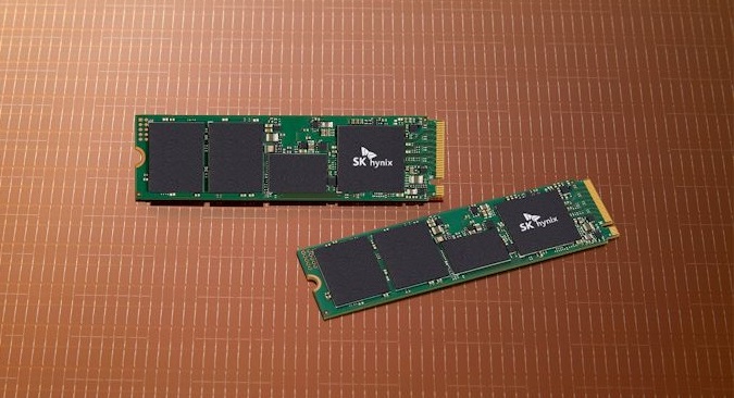
SK Hynix announced this week that it had started volume production of its 238-layer TLC NAND memory. The new device promises higher bit density and lower NAND bits cost for the manufacturer and enables ultra-high-performance SSDs as it features a very high interface speed of 2400 MT/s.
SK Hynix's first 238-layer 3D TLC NAND device has a 512 Gb capacity (64 GB). It has a number of benefits when compared to its 176-layer predecessor, including a 34% higher manufacturing efficiency (i.e., smaller die size, lower usage of materials, and expensive process steps, etc.), a 21% lower power consumption during read operations thanks to the ONFI 5.0 interface with the NV-LPDDR4 signaling method, and a 2400 MT/s interface transfer rate, which is a 50% increase.
The latter is perhaps the most crucial advantage of the new memory chip for PC enthusiasts, as contemporary and upcoming client SSDs with a PCIe 5.0 x4 interface need high-speed memory devices to saturate it. Currently, available 3D NAND with a 1600 MT/s interface can only enable drives with an approximately 10 GB/s sequential read/write speed, but to get to 12.5 GB/s and even higher, one needs to either use high-speed memory or use more memory devices and an appropriate controller.
SK Hynix's 238-layer 3D TLC NAND uses string stacking to join a pair of 119-layer decks as well as charge-trap, CMOS under Array (CuA) architecture, which places NAND logic under the 3D NAND memory cells array to reduce die size and costs. This is why SK Hynix calls this architecture 4D NAND.
| SK hynix 3D TLC NAND Flash Memory | ||
| 238L | 176L | |
| Layers | 238 | 176 |
| Decks | 2 (x119) | 2 (x88) |
| Die Capacity | 512 Gbit | 512 Gbit |
| Die Size (mm2) | 35.58mm2 | ~47.4mm2 |
| Density (Gbit/mm2) | ~14.39 | 10.8 |
| I/O Speed | 2.4 GT/s (ONFi 5.0) |
1.6 GT/s (ONFI 4.2) |
| CuA / PuC | Yes | Yes |
SK Hynix is the third major maker of NAND flash memory to start production of 3D NAND with over 200 layers. SK Hynix said that one of the large smartphone makers was about to complete compatibility tests with its 238-layer 3D NAND devices. Once it does, SK Hynix will start shipping these memory chips to the handset producer. Eventually, these devices will be used for PCIe 5.0 SSDs and high-capacity server drives, the company said.
"SK Hynix has developed solution products for smartphones and client SSDs which are used as PC storage devices, adopting the 238-layer NAND technology, and has moved into mass production in May," a statement by SK Hynix reads. "Given that the company secured world-class competitiveness in price, performance, and quality for both 238-layer NAND and the previous generation 176-layer NAND, we expect these products to drive earnings improvement in the second half of the year."
Source: SK Hynix


5 Comments
View All Comments
meacupla - Thursday, June 8, 2023 - link
I'm sorry, but that "4D NAND" marketing name is hilarious.Technically impressive, but marketing ruining things as usual.
Memo.Ray - Friday, June 9, 2023 - link
Everyone knows that once you pass the 199th layer you enter the 4th dimension!b0e57d1d - Friday, June 9, 2023 - link
We'll have 5D, 6D, 8D, and 16D soon!!FunBunny2 - Sunday, June 11, 2023 - link
nanu nanulemurbutton - Monday, June 12, 2023 - link
Well, it's 4D technically. Time is a dimension and SK Hynix's 238-layer 3D TLC NAND cannot exist without the time dimension. In fact, none of us can exist without it.