SK hynix Reveals DDR5 MCR DIMM, Up to DDR5-8000 Speeds for HPC
by Gavin Bonshor on December 8, 2022 12:00 PM EST
One of the world's biggest semiconductors and manufacturers of DRAM, SK hynix, has unveiled it has working samples of a new generation of memory modules designed for HPC and servers. Dubbed Multiplexer Combined Ranks (MCR) DIMMs, the technology allows high-end server DIMMs to operate at a minimum data rate of 8 Gbps, which is an 80% uptick in bandwidth compared to existing DDR5 memory products (4.8 Gbps).
Typically, the most common way to ensure higher throughput performance on DIMMs is through ever increasing memory bus (and chip) clockspeeds. This strategy is not without its drawbacks, however, and aiming to find a more comprehensive way of doing this, SK hynix, in collaboration with both Intel and Renesas, has created the Multiplexer Combined Rank DDR5 DIMM.
Combining Intel's previously-unannounced MCR technology for its server chips and Renesas's expertise in buffer technology, SK hynix claims that their DDR5 MCR DIMM has 66% more bandwidth than conventional DDR5 DIMMs, with an impressive 8 Gbps/pin (DDR5-8000) of bandwidth. SK hynix themselves claim that the MCR DIMM will be 'at least' 80% faster than what's currently out there DDR5-wise, but it doesn't quantitate how it reaches this figure.
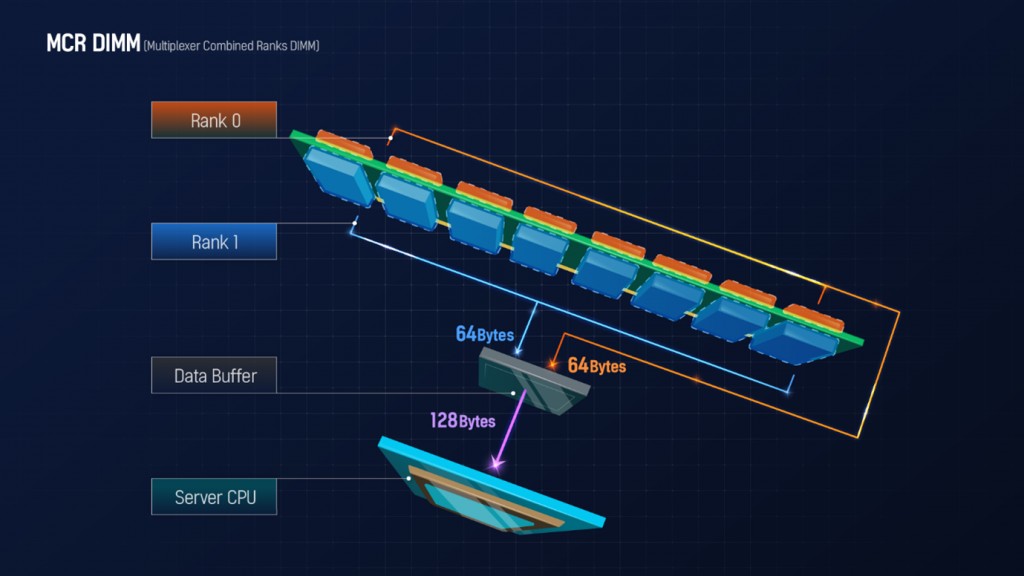
The technology behind the MCR DIMM is interesting, as it enables simultaneous usage of two ranks instead of one, in essence ganging up two sets/ranks of memory chips in order to double the effective bandwidth. Unfortunately, the details beyond this are slim and unclear – in particular, SK hynix claims that MCR "allows transmission of 128 bytes of data to CPU at once", but looking at the supplied DIMM photo, there doesn't seem to be nearly enough pins to support a physically wider memory bus.
More likely, SK hynix and Intel are serializing the memory operations for both ranks of memory inside a single DDR5 channel, allowing the two ranks to achieve a cumulative effective bandwidth of 8Gbps. This is supported by the use of the Renesas data buffer chip, which is shown to be on the DIMM in SK hynix's photos. Conceptually, this isn't too far removed from Load Reduced DIMMs (LRDIMMs), which employs a data buffer between the CPU and memory chips as well, though just how far is difficult to determine.
More curious, perhaps, is that this design puts a great deal of faith into the ability of the physical memory bus and host controller (CPU) to be able to operate at DDR5-8000 (and higher) speeds. Normally the bottleneck in getting more memory bandwidth in server-grade systems is the memory bus to begin with – having to operate at slower speeds to accommodate more memory – so going a route that requires such a fast memory bus is definitely a different approach. In either case, the ability to run DIMMs at DDR5-8000 speeds in a server would be a significant boon to memory bandwidth and throughput, as that's often in short supply with today's many-core chips.
As SK Hynix has partnered up with Intel via its MCR technology and using buffer technology from Renesas, MCR would seem to be an Intel-exclusive technology, at least to start with. As part of SK hynix's press release, Intel for its part stated that they "look forward to bringing this technology to future Intel Xeon processors and supporting standardization and multigenerational development efforts across the industry.” In the interim, this appears to be a technology still under active development, and SK hynix is not publishing anything about availability, compatibility, or pricing.
While SK Hynix hasn't gone too much into how MCR DIMM is twice as fast as conventional DDR5 memory, this product is designed for the high-performance computing (HPC) and server industries, and it's unlikely we'll see MCR DIMMs in any form on consumer-based systems. We expect to learn more in the not-too-distant future.
Source: SK Hynix


20 Comments
View All Comments
kpb321 - Thursday, December 8, 2022 - link
I assume the 128b is not because it's using a wider memory bus but because the memory controller is using that for addressing both ranks at one time. So it's not two independent 64bit memory channels being interleaved but one 128bit memory address being read over a 64bit bus so Rank 0 and Rank 1 are always reading from the same addresses. Two independent buses would be more flexible but probably harder to implement.I wonder what this does to max memory capacity. Presumably having a buffer chip like LRDIMMS would help support more dimms per channel and therefore memory capacity but running the memory bus at such high speed might counteract that.
mode_13h - Monday, December 26, 2022 - link
> I assume the 128b is not because it's using a wider memory busWhere did you get 128 bits? Neither the article nor the original press release said anything about 128 bits. Then, you just dig yourself a deeper hole talking about 64-bit memory channels and "128 bit memory address"... WTF?
Gavin caused a lot of confusion with the statement: "there doesn't seem to be nearly enough pins to support a physically wider memory bus." *Obviously*, they don't mean 128 byte-wide bus, as that would mean having 1024 pins per channel! Duh.
DDR5 uses a minimum burst size of 64 bytes. That's implemented as a sequence of 16 cycles of 32 bits per cycle, because each DDR5 DIMM has 2x 32-bit channels. So, what they're saying is that by multiplexing two ranks, MCR increases that burst size to 128 bytes.
That could pose issues, from the CPU's point of view, because CPU cache lines are 64 bytes, hence the natural transaction size would be only half of what MCR would support. In the worst case, this could mean half of each burst is wasted, if the transfers to a given channel are all non-consecutive. That's a big deal.
> I wonder what this does to max memory capacity.
Depends on how many ranks you can fit on one of these DIMMs. If you can make a quad-ranked DIMM, with each pair being multiplexed to appear as a single rank, then you'd double the max capacity per DIMM (assuming DDR5 doesn't already support quad-ranked RDIMMs - does anyone know?). Otherwise, no change.
MobiusPizza - Thursday, February 16, 2023 - link
the article did say 128 bytes, even the author wasn't sure how"Unfortunately, the details beyond this are slim and unclear – in particular, SK hynix claims that MCR "allows transmission of 128 bytes of data to CPU at once", but looking at the supplied DIMM photo, there doesn't seem to be nearly enough pins to support a physically wider memory bus."
Kevin G - Thursday, December 8, 2022 - link
I wonder what latency impact is. I would presume something small since this piggy backs off of LR-DIMM topology. Similarly I wonder this does to the various subtimings on the module.Presuming these work on Genoa chips (big if given the parties involved), that'd permit 768 GByte/s of memory bandwidth per socket. That's rather impressive.
onewingedangel - Thursday, December 8, 2022 - link
I read it as 128-bit wide DDR5-4000 to an on module buffer that then transfers to the CPU over a 64-bit DDR5-8000 bus - thus lowering required pin count compared to standard DDR5.Jp7188 - Wednesday, January 4, 2023 - link
That's the way I read it too. It sounds like DDR5 buses are moving to speeds the chips can't supply, so they are using two slower chips to feed a buffer that then transfers over a traditional (higher speed) DDR5 bus. If true, all Intel (and AMD) need to do is support DDR5-8000.meacupla - Thursday, December 8, 2022 - link
so does the mobo need to support MCR DIMMs, or will it work in any mobo that supports DDR5?Because if MCR only works in MCR mobos, then I don't see why they wouldn't just use a wider memory bus from the server level CPU. Like give it 32 channels.
Kevin G - Sunday, December 11, 2022 - link
Motherboard complexity goes up as more channels are added. The 12 channels Genoa has is on the upper limits of what is feasible without going to fully buffered memory/CLX.mode_13h - Monday, December 26, 2022 - link
> The 12 channels Genoa hasSince each DDR5 DIMM has 2x 32-bit subchannels, Genoa should technically have a 24-channel memory subsystem. Just sayin'.
The Von Matrices - Sunday, December 11, 2022 - link
This doesn't add any more traces on the motherboard, and the memory slots would be the same. However, like LRDIMMs and ECC, the memory controller on the CPU has to support it, which I doubt AMD and especially Intel will do on anything but their most expensive server CPUs.