GlobalFoundries To Spend Billions: Doubling Fab 8, Creating New Fab in NY
by Dr. Ian Cutress on July 19, 2021 11:36 AM EST- Posted in
- GlobalFoundries
- Semiconductors
- Fab 8
- Malta

Today at a private GlobalFoundies event, CEO Tom Caulfield accompanied by Senate Majority Leader Chuck Schumer, announced that the company is set on expansion. At the heart of this new initiative is a doubling of Fab 8, GF’s leading manufacturing facility, at the cost of around $1B. Accompanying this is the disclosure that GF is going to build another manufacturing facility close to Fab 8, in Malta NY, as part of a Private-Public partnership. Details of the new facility were not given.
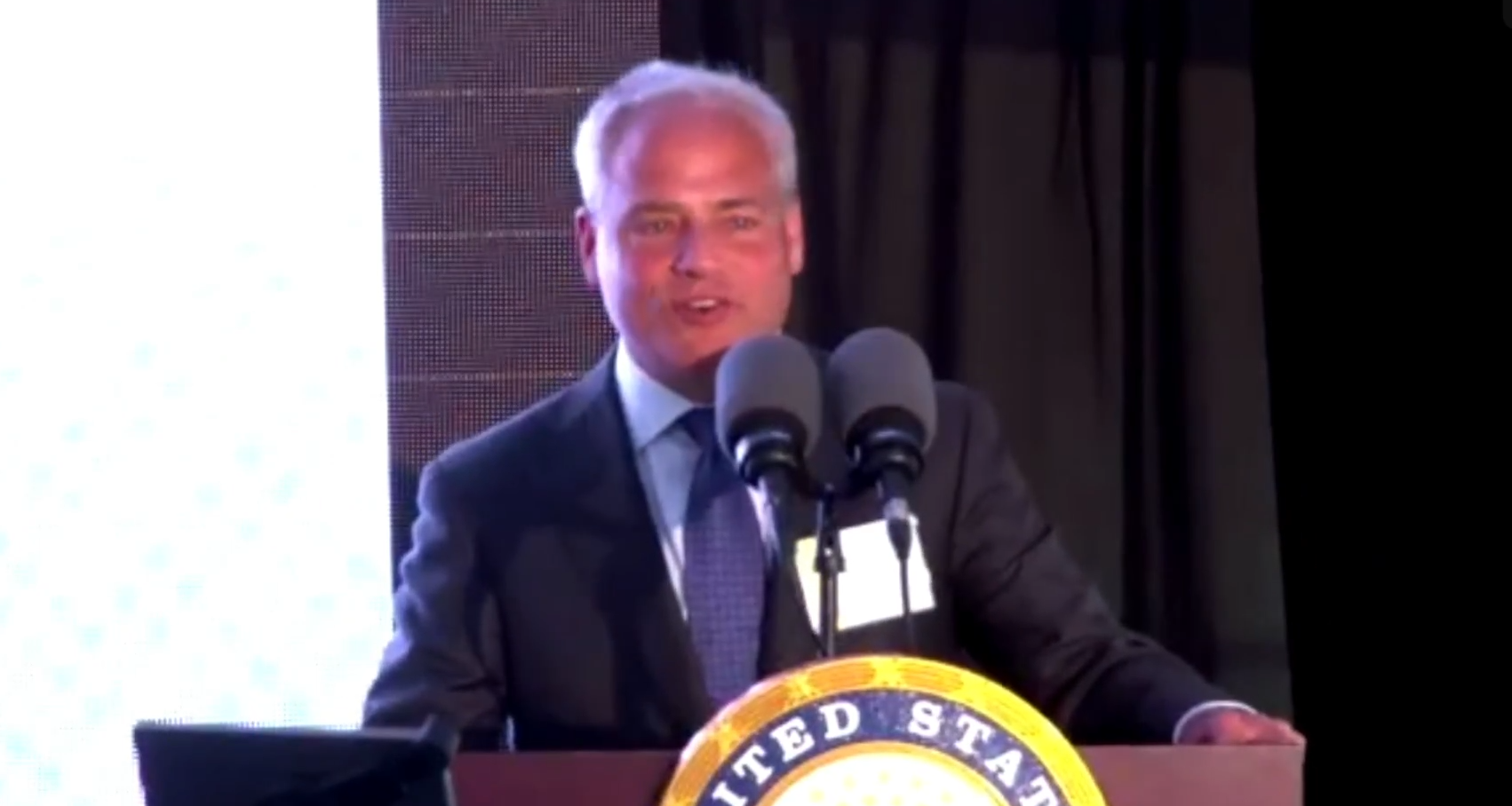
CEO Tom Caulfield
GlobalFoundries is a contract manufacturer of microprocessors, focusing on adjacency technologies from 12nm and larger geometries. While most column inches are spent discussing the leading-edge manufacturing at GF’s competitors, in a discussion with the CEO we were told that GF addresses around 70% of the semiconductor market and in the current climate is currently running all of its facilities at maximum production.
GF has three main fabs in Malta NY, Dresden Germany, and Singapore – all three are running at maximum output, and GF recently announced a new plant in Singapore capable of 450K wafers per year. Tom Caulfield told us prior to that announcement that the Malta fab is around two-thirds full of equipment, Dresden is at about half, but Singapore is full, hence the new Singapore fab. In March GF announced a $1.4B expansion divided equally between the three sites, with Production capacity is expected to increase by 13% this year and by 20% next year as a result of the increased funding. Today’s announcement commits to adding additional machines at Malta to scale out to the space already there, for another 150k wafers per year, at a cost of $1B.

New website with the new branding. They should have put 'Moore'
The other element of the announcement is the new fab in Malta. The deployment of a new facility, especially at scale, costs billions. GlobalFoundries today acknowledges that it will take billions, citing the US government’s desire to increase national manufacturing in light of the global scale and building more on American soil. Exactly how GF will implement a new facility has not been disclosed – no timeline, no costs, no information about where the funding is coming from, or what process nodes will be manufactured on-site. It was announced that it would be a private-public partnership, developing chips for high-growth areas such as automotive, 5G, and IoT. The fab is set to create 1000 technical jobs and another few thousand in ancillary positions in the local area to support it. Discussions were also made in light of the semiconductor supply chain, and the need to invest and evolve that part of the business alongside manufacturing improvements. Senator Schumer spoke about the need to pass grow semiconductors, holding up a bag of chips alongside a wafer.

These announcements are part of a train of recent disclosures and talk about GlobalFoundries. Last week it was rumored that Intel was seeking to acquire GF for $30 billion, however today GF announced a complete logo change and rebranding of the business, which doesn’t tend to occur if a company is in the process of acquisition talks. Alongside this, GF is expected to bring forward its Initial Public Offering (IPO) from 2022 to late 2021. The company is currently owned wholly by the Emerati state holding company Mubadala, and the IPO is on the back of some growth of GF in light of the high semiconductor demand environment. GlobalFoundries expects 2021 revenue to be around $6.2 billion, a +9% growth over 2020.
Official Press Release from GlobalFoundries
Related Reading
- GlobalFoundries To Build New 450K Wafer-per-Year Fab in Singapore
- AMD and GlobalFoundries Update Wafer Supply Agreement: Orders Through 2024, Now Non-Exclusive
- GlobalFoundries Upgrades for Silicon Photonics in Quantum Computers
- GlobalFoundries to Invest $1.4B in Expansion, Potential Earlier IPO
- GlobalFoundries' 22FDX with MRAM is Ready
- GlobalFoundries and SiFive to Design HBM2E Implementation on 12LP/12LP+
- GlobalFoundries and TSMC Sign Broad Cross-Licensing Agreement, Dismiss Lawsuits


74 Comments
View All Comments
shabby - Monday, July 19, 2021 - link
Still stuck at 12nm? Are they really not going to spend any money on improving that? Tsms/samsung just need to undercut them a bit and they'll start losing customers.psychobriggsy - Monday, July 19, 2021 - link
Maybe they will license Samsung's 7nm or 5nm, just like they licensed the 14nm, but that would be expensive, especially with the need for EUV hardware.Maybe there's a lot of money still in 12nm of various forms. Not everybody needs cutting edge, but you need to follow your competition at some point.
dwillmore - Monday, July 19, 2021 - link
Every Ryzen chip sold has TSMC chiplet(s) and an GF I/O chip. Looking at the layout of the chip packages, the I/O chip isn't limiting the design--you need a lot of surface area for the I/O, so going denser with the logic doesn't buy you much more. Possilby, they could put more L3 on there, but they're surface area/IO bound on those chips. Why pay for a process that doesn't buy you anything?Possibly it would make sense to make a more power efficient chip for mobile Ryzen parts? But at that point, might as well integrate the I/O onto the main die and be done with it.
Currently, every fab everywhere is at capacity--all the way back to micron sized features. Pay for capacity not process improvement right now. A year or two from now that may change, but there's always going to be a use for those older fabs.
nandnandnand - Monday, July 19, 2021 - link
AMD is about to ditch 12nm and use TSMC's 6nm for Rembrandt and I/O dies. But they could also use GloFo's newer 12LP+, e.g. for "Monet" quad-core Zen 3 APUs. And AMD will probably continue making various 12nm parts for the embedded market.whatthe123 - Tuesday, July 20, 2021 - link
GF's i/o chips take up quite a bit of power. In chips with massive amounts of cores like milan it can take up as much power as the cores themselves. I doubt they will be able to continue scaling IPC and/or core count if they stick with global foundries, at least at the enterprise level.dwillmore - Tuesday, July 20, 2021 - link
The I/O chips use the power they do mostly because of the interfaces they provide and that will not vary with process geometry. It takes a certain amount of power to run a PCI-E 4.0 bus, same for SDRAM, etc. The only amount that varies a bit is the logic behind those protocols and the cache. Cache is mostly leakage and that doesn't improve with smaller processes.There's not much to gain with a smaller process geometry and it will increase the cost of the I/O dies.
FreckledTrout - Tuesday, July 20, 2021 - link
One could integrate the chipset into the IO die to keep the surface area high.dwillmore - Tuesday, July 20, 2021 - link
These chips are SoCs. The chipset *is* integrated into the I/O die. At least on the desktop parts. I don't know about the server ones.whatthe123 - Tuesday, July 20, 2021 - link
If that were the case the I/O wouldn't take so much power compared to similar core count icelake chips.Anandtech already did review on them and the I/O uses a significant amount more power than chips with the same platform features, and another revision where they were able to improve performance with more power delivery, so even current cores have performance headroom but are held back by package power.
dotjaz - Wednesday, July 21, 2021 - link
That's definitely not the case for the high volume desktop processors. 95W is easily achievable, so the mere extr 5W IOD cost can't be limiting anything.