Samsung Launches Single-Chip uMCP Packages with LPDDR4X DRAM & UFS 3.0 Storage
by Anton Shilov on October 24, 2019 9:00 AM EST
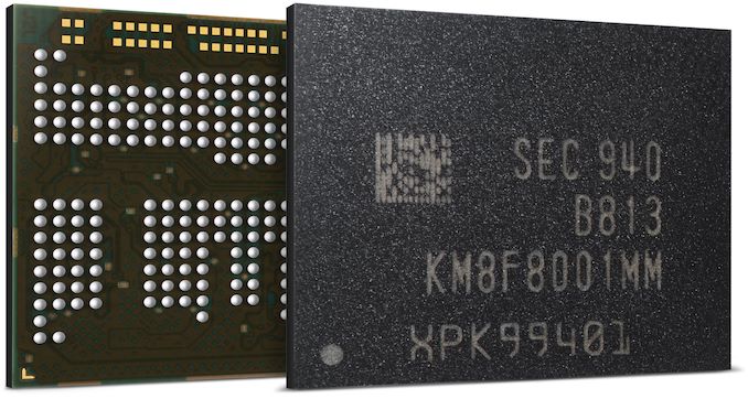
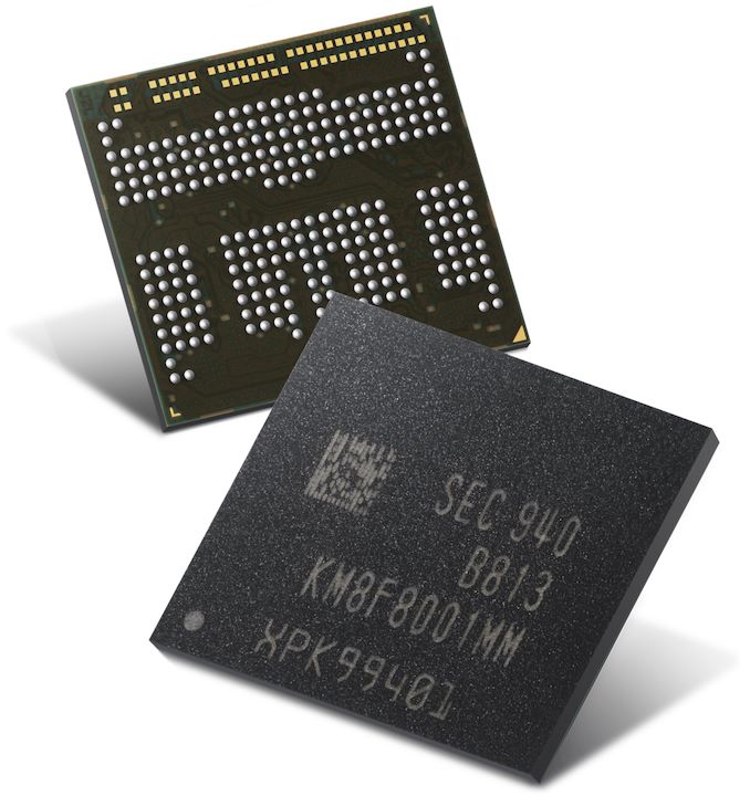
Samsung has introduced a new lineup of all-in-one memory packages for smartphones that integrate both DRAM and storage. The latest generation of uMCP devices now feature up to 12 GB of LPDDR4X DRAM as well as NAND flash storage with a UFS 3.0 interface, thus providing high performance memory for mainstream handsets in a cost-effective form-factor.
Samsung’s UFS-based multichip packages (uMCPs) integrate 10 GB or 12 GB of LPDDR4X-4266 memory (made using the company’s 2nd Generation 10nm-class process technology) as well as NAND flash storage featuring a UFS 3.0 interface. Since both new uMCP modules incorporate four DRAM devices, they will allow the latest SoCs with quad-channel LPDDR4X memory controllers to reach up to 34.1 GB/s memory bandwidth. Meanwhile on the NAND side of matters, Samsung's official announcement doesn't list what storage capacities will be available there, but the company has commented that they can provide the uMCPs in a variety of capacities.
Meanwhile, the new uMCP devices are also mechanically compatible with Samsung's previous-generation 8GB uMCPs, utilizing the same 254FBGA package.
| Samsung's uMCPs w/ UFS 3.0 Storage | ||||
| DRAM | NAND | |||
| 10 GB | 2×24 Gb (3 GB) + 2×16 Gb (2 GB) devices | eUFS 3.0 | ||
| 12 GB | 4×24 Gb (3 GB) devices | eUFS 3.0 | ||
Today, only high-end smartphones come equipped with 12 GB of LPDDR4X memory, but Samsung expects its new uMCPs to enable upcoming mid-range handsets to feature 10 GB or 12 GB of DRAM. The new uMCP devices are already in mass production, so expect smartphones launching in the coming months to use them.
Samsung did not disclose pricing of its 10 GB uMCP and 12 GB uMCP chips, but expect them to cost in accordance with prices of DRAM and storage.
Related Reading:
- Samsung Begins Mass Production of 12 GB LPDDR4X for Smartphones
- Samsung Develops Smaller DDR4 Dies Using 3rd Gen 10nm-Class Process Tech
- Samsung Starts Production of 8 Gb DDR4-3600 ICs Using 2nd Gen 10nm-Class Tech
- Samsung Starts Production of 1 TB eUFS 2.1 Storage for Smartphones
Source: Samsung


30 Comments
View All Comments
shabby - Thursday, October 24, 2019 - link
Do they ever announce the pricing of these kind of chips?drexnx - Thursday, October 24, 2019 - link
probably depends on quantity, configuration, how much other stuff you buy from Samsung LSI, how long of a delivery you'll accept, etc.Raqia - Thursday, October 24, 2019 - link
It's pretty remarkable that desktops and even laptops still sport bulky DIMMs and SSDs when these get the job done with better latency and lower power in a tiny fraction of the area. If Windows on ARM gains purchase or Apple shifts to arm as rumored with the MacBook Air in 2020, it should usher in significant form factor changes for many popular markets.IntelUser2000 - Thursday, October 24, 2019 - link
Ok, when you want to make something people can upgrade, you have to compromise. The connectors have to be robust enough to withstand many cycles, and that'll change things quite drastically.If you integrate things you can make it lower power and sometimes even lower latency. But the mobiles are much higher latency anyway. Geekbench 4 memory scores show 40-60ns for desktop Intel platforms and Apple A12 gets 110ns.
If you want to cater to the upgrade market then such "bulky" DIMMs and SSDs will continue to exist.
Kevin G - Thursday, October 24, 2019 - link
It is interesting actually looking through some of the manuals to realize just how few remove/add cycles parts are rated for. CPU sockets are roughly around 15 generally. The serves most customers as there are few upgrades and only one performed if any. However, that is a relatively low number of cycles to support.Platform latency is generally dependent upon the platform. See the difference between AMD and Intel desktop chips for example. Apple in mobile is doing very aggressive power management and factors like putting the memory bus to sleep and relaying on the DRAM's self refresh is a thing. These add latency vs. a desktop whose memory bus is expected to be always on.
The condensation of equipment makes sense in mobile but for desktops and servers, upgradbility is still important that the extra bulk is worth it.
Raqia - Thursday, October 24, 2019 - link
Highly integrated SoCs are simply not in favor for desktop performance envelopes but very well could be if tuned for such purposes due to better performance and lower cost. There really will be performance improvements for accelerators like GPUs when SoC memory bandwidth improves and copying data over a bus to a separate pool of memory becomes moot for instance. The cost of replacing the entire SoC with ram and storage should be cheaper than more modular upgrades and give bigger aggregate performance benefits.IntelUser2000 - Thursday, October 24, 2019 - link
It's not just that. If you want upgradeability, you need standards. Standards take time to implement, whether its your own, or to make it work as an ecosystem. LGA1151 is a standard Intel decided to make for their chips. There are certain size requirements they have to meet.It's true that absolute number of remove/add cycles may be low. But it still needs a degree of robustness not existing in an integrated part. Sockets also take up extra space. Ultrabooks don't have it because if you want the entire laptop, folded to be 15mm thin, then BGA is the only way to go.
Integrated solutions don't need to care about this. They can change depending on the need.
Raqia - Thursday, October 24, 2019 - link
There's a great quote from Orwell's Animal Farm by Benjamin the Donkey that I think applies to protocols enabling modular upgrades: "God gave me a tail to keep off the flies. But I'd rather have had no tail and no flies." I think while general bus protocols will continue have a place in the future of computing hardware, both the excess overhead of needlessly general protocol traffic as well as the modular paradigm of design will impede performance for accelerators that can be integrated on an SoC that share a pool of very fast memory with the CPU. I'd rather the likes of Apple or Qualcomm give me a whole new SoC on a new cutting node every few months with upgrades to the entire assemblage than piecemeal assemble it together myself sacrificing both speed, power efficiency, and at higher cost.name99 - Thursday, October 24, 2019 - link
Amen brotherRaqia - Thursday, October 24, 2019 - link
As cost goes down and performance plateaus, upgrades that were common when prices were high and improvements were rapid at the socket level become moot. I had a past infatuation with upgrading individual parts in the old modular model which is waning in favor of more integrated upgrades as SoCs are becoming better at a much faster clip than higher power envelope parts, and I think will soon displace more traditional desktop layouts in much higher performance envelopes. Many off SoC accelerators will probably go the way that separate FPUs did in the 90's when TSMC's 5nm processes allows for ~15B transistors on a commercial SoC and ram stacking technologies eliminate this performance bottleneck from consumer systems. Memory absolutely doesn't have to be higher latency in theory as wire distances are simply much lower when it is wired to the package or connected by TSVs.I'm happier to pay ~$700 a pop for a new slim PCB with an SoC at a leading edge process with everything you find in a typical PC built in rather than ~$1,000 for a CPU+Mobo+GPU with upgradeable DIMMs + and PCIe slots with approximately $500 of added cost per upgrade of CPU, RAM, or GPU with much unwanted bulk, heat, and bus interface distances. (You typically wouldn't find a cellular modem there either.)