SK Hynix Announces 3.6 Gbps HBM2E Memory For 2020: 1.8 TB/sec For Next-Gen Accelerators
by Ryan Smith on August 12, 2019 10:00 AM EST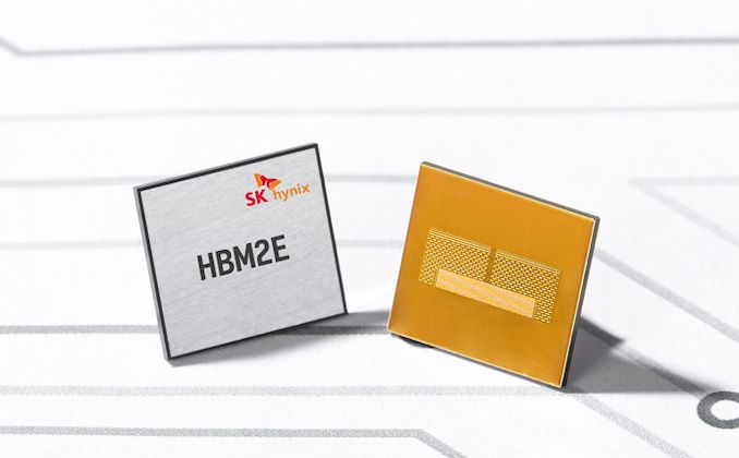
SK Hynix this morning has thrown their hat into the ring as the second company to announce memory based on the HBM2E standard. While the company isn’t using any kind of flash name for the memory (ala Samsung’s Flashbolt), the idea is the same: releasing faster and higher density HBM2 memory for the next generation of high-end processors. Hynix’s HBM2E memory will reach up to 3.6 Gbps, which as things currently stand, will make it the fastest HBM2E memory on the market when it ships in 2020.
As a quick refresher, HBM2E is a small update to the HBM2 standard to improve its performance, serving as a mid-generational kicker of sorts to allow for higher clockspeeds, higher densities (up to 24GB with 12 layers), and the underlying changes that are required to make those happen. Samsung was the first memory vendor to announce HBM2E memory earlier this year, with their 16GB/stack Flashbolt memory, which runs at up to 3.2 Gbps. At the time, Samsung did not announce a release date, and to the best of our knowledge, mass production still hasn’t begun.
Not to be left behind, SK Hynix is now also readying their own HBM2E memory. In terms of performance, SK Hynix says that their memory will be able to clock at up to 3.6 Gbps/pin, which would give a full 1024-pin stack a total of 460GB/sec of memory bandwidth, and in the process the lead for HBM2E memory speeds. And for more advanced devices which employ multiple stacks (e.g. server GPUs), this means a 4-stack processor could be paired up with as much as 1.84TB/sec of memory bandwidth, a massive amount by any measure. Meanwhile their capacity is doubling, from 8 Gb/layer to 16 Gb/layer, allowing a full 8-Hi stack to reach a total of 16GB. It’s worth noting that the revised HBM2 standard actually allows for 12-Hi stacks, for a total of 24GB/stack, however we’ve yet to see anyone announce memory quite that dense.
Given SK Hynix’s announcement, it’s interesting to note just how quickly HBM2 memory speeds have ramped up here: HBM2 vendors could barely do 1.9 Gbps 24 months ago, and now we’re looking at a near doubling of memory speeds in 3 years. This is a rather significant gain in a short period of time, especially with only a minor revision to the HBM2 spec being required. That said, I remain curious as to how SK Hynix (and Samsung) are going to deal with the heat of an 8-Hi stack running at those clocks; the HBM design philosophy is wide-and-slow, and 3.6 Gbps arguably isn’t so slow.
With their HBM2E memory set to go into mass production in 2020, SK Hynix expects the new memory to be used on “supercomputers, machine learning, and artificial intelligence systems that require the maximum level of memory performance.” All of these are distinctly high-end applications where HBM2 is already being heavily used today, so HBM2E is a natural extension to that market. At the same time, it’s also a reflection of the price/margins that HBM2 carries. HBM2 has remained (stubbornly) high-priced well after its release – a situation that memory manufacturers seem to be perfectly content with – and we’re not expecting HBM2E to change that. So expect to see SK Hynix’s HBM2E memory remain the domain of servers and other high-end equipment.
Source: SK Hynix


23 Comments
View All Comments
Targon - Monday, August 12, 2019 - link
Outside of professional applications, for a GPU, the limitation is currently on GPU performance, and isn't being held back all that much by the existing HBM2 or GDDR6 standards. Sure, faster memory will result in some benefits, but for the difference in cost, the benefits may not be worth it. That is the big question, and I would hope that AMD and/or NVIDIA would show the performance difference of a given GPU with GDDR6 vs HBM2 or HBM2E. If you get 5fps better with the HBM2E memory but it raises the cost of a video card by $200, people won't want to go for it.extide - Monday, August 12, 2019 - link
Well, actually a lot of recent AMD cards could really use more B/W. The Radeon VII has plenty but it had to resort to 4 stacks of HBM -- if we could provide 920GB/sec using only 2 stacks, it would be really handy.guidryp - Monday, August 12, 2019 - link
It's not like the Radeon VII actually needs that much BW. It gets outperformed by the RTX 2080 that only has about half that (448 GB/sec).I doubt we will see HBM except at the VERY high end of GPUs going forward, since they are keeping the prices high.
mdriftmeyer - Monday, August 12, 2019 - link
He's talking about computation crunching, not gaming.extide - Monday, August 12, 2019 - link
Radeon VII performance still scales with memory bandwidth -- so it's hard to say. Nvidia's arch is totally different so you can't really compare it directly to them. Navi also seems to hit a memory b/w wall around 2100Mhz as well.rhysiam - Tuesday, August 13, 2019 - link
I'm with @extide here - AMD cards seriously struggle with memory bandwidth. Look at OCing reviews of the 5700XT, it hardly scales at all with core frequency OCing, but scales healthily with memory clock (what little you can extract from it, anyway). I suspect a 5700 XT with 920GB/s from two stacks of this new HBM would be quite a bit faster.JasonMZW20 - Tuesday, August 13, 2019 - link
Compute workloads are uncompressed, so require a ton of memory bandwidth. This is why Vega 20 steamrolls Vega 10 in compute.Graphics workloads, however, benefit from memory compression, so there's a diminishing return with memory OC in GPU-limited scenarios (higher resolutions).
What people are mixing up as a memory bandwidth limitation though is during overclocking, they tend to increase the power limit of the GPU. Of course, allowing the GPU to reduce its power throttling will improve performance.
What needs to be done is a run at stock clocks, stock power limit, and a comparison between 14Gbps and 15Gbps (Navi) or 1100-1250MHz HBM on Vega 20. If there's no real gains, there isn't a memory bandwidth limitation. If you see gains outside of the margin of error but below 5%, I'd call it marginal. When you stsrt seeing upwards of 10% performance as you see in APUs using faster DDR4 system memory, then it's safer to declare that memory bandwidth is a limiting factor.
JasonMZW20 - Tuesday, August 13, 2019 - link
1000-1250MHz on Vega 20*Skeptical123 - Tuesday, August 13, 2019 - link
lol what are you talking about "It's not like the Radeon VII actually needs that much BW". The only reason AMD went with HBM memory in the first place a few years ago was a costly "last ditch" effort to get close to Nvida cards performance. There GPU could not meet snuff so AMD had to give them an "edge" which was the HBM. Which at the time was widely reported killed their margins on the card. HBM is still not cheap and while AMD recently has had a good run there still a reason why AMD is not using GDDR6.DanNeely - Monday, August 12, 2019 - link
Except at the race to the bottom end, it's been a really long time since we've had GPUs bottlenecked by memory IO in normal gaming use. Better texture compression and more total rendering time being spent doing things that don't need more textures are helping here a lot.Some compute uses can do so, and more can benefit from the higher max capacity it allows; which is why NVidia eschews it in consumer cards while offering it in some workstation/compute cards. AMD's made more use of it consumerside; but even they switched back to GDDR6 for RX5700 at 50% of Radeon VI's bandwidth without problem.
Pushing higher per stack speeds and capacities to let cards get away with fewer stacks might help push costs down enough to make it more mainstream if GDDR ever does run out of room to grow; especially if the smaller stack count allows replacing big expensive interposers with tiny bits of silicon like with Intel's EMIB. That said in the medium term I'm not really expecting to see it in the consumer end much if at all - and only to the extent that consumer halo products are rebadged workstation/compute designs.