Investigating NVIDIA's Jetson AGX: A Look at Xavier and Its Carmel Cores
by Andrei Frumusanu on January 4, 2019 11:00 AM EST- Posted in
- NVIDIA
- SoCs
- Xavier
- Automotive
- Jetson
- Jetson AGX
Today’s piece is a bit of an unusual review; NVIDIA’s new Jetson AGX embedded system kit isn’t really a device platform we’re expecting the average reader to think about, much less buy. NVIDIA’s shift over the last few years from offering consumer grade Tegra chipsets to more specialised silicon applications isn’t any more evident than in the new Tegra Xavier which powers the Jetson AGX. While the board's capabilities certainly fall outside of the use-cases of most consumers, it still represents a very interesting platform with a lot of functionality and silicon IP that we don’t find in any other device to this day. So when NVIDIA reached out to offer us a sample, we decided to have a go at assembling a high-level overview of what the board and the new Xavier chip can do.
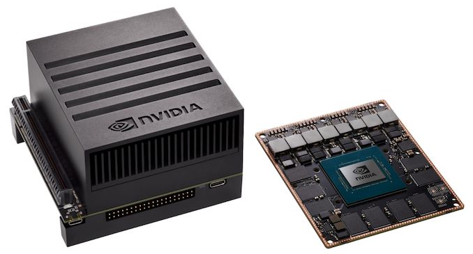
First of all, we have to describe what this actually is. The Jetson AGX is a full-fledged small form-factor computer / embedded system, with the form of the whole unit not any bigger than 105x105mm. The AGX module itself is designed to be a complete commercial off the shelf (COTS) system for use in finished products, with NVIDIA aiming it at AI (read: neural networking) centric use cases such as robotics and industrial automation. Jetson boards typically occupy the small-to-mid volume end of the market, showing up in one-off products and items with limited production runs, where it doesn't make sense for a manufacturer to develop and deploy their own custom hardware.
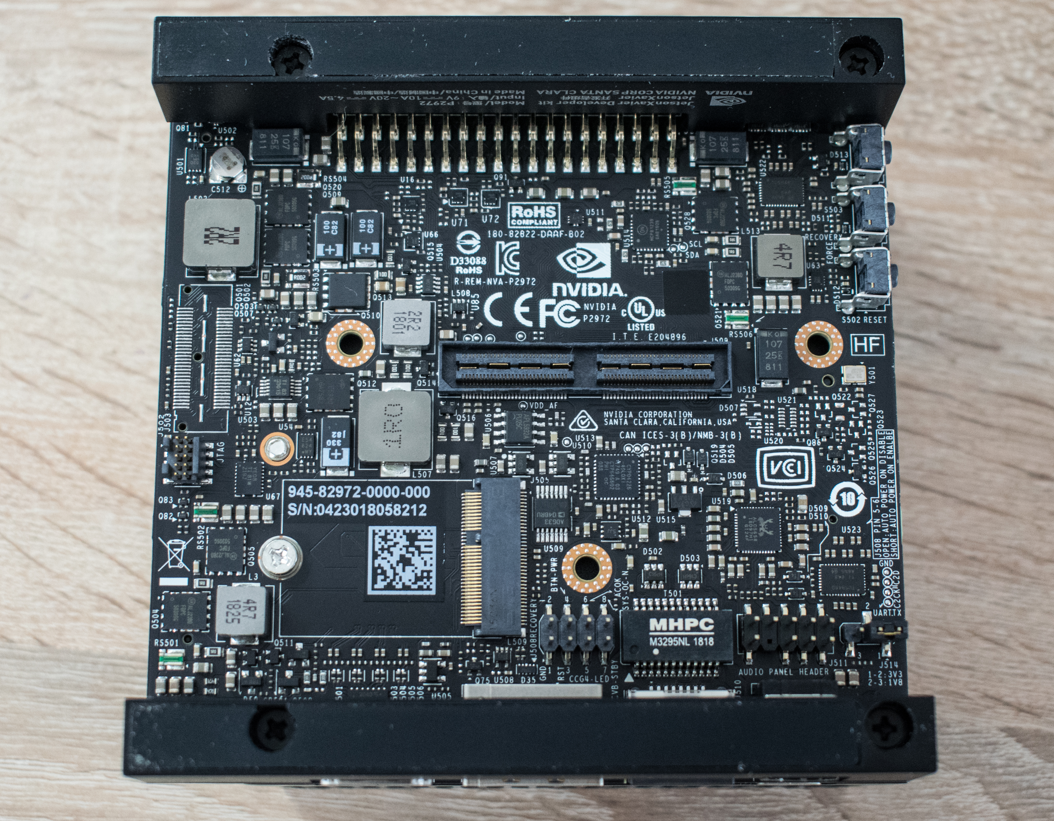
But of course the bare module is only half the story. You can't do development against a bare module, and this is where NVIDIA's complete Jetson AGX development kit comes in. The AGX dev kit comes with everything needed to run a single module, including a power supply, a heatsink, and more important of all, a breakout board. The breakout board offers various I/O headers and ports, ranging from your standard double USB-C 3.1 ports, HDMI connectors and Gigabit Ethernet ports, to more specialised connectivity such as MIPI CSI-2 connectors for camera connectivity and a range of typical development board headers such as a 40 pin GPIO connector.
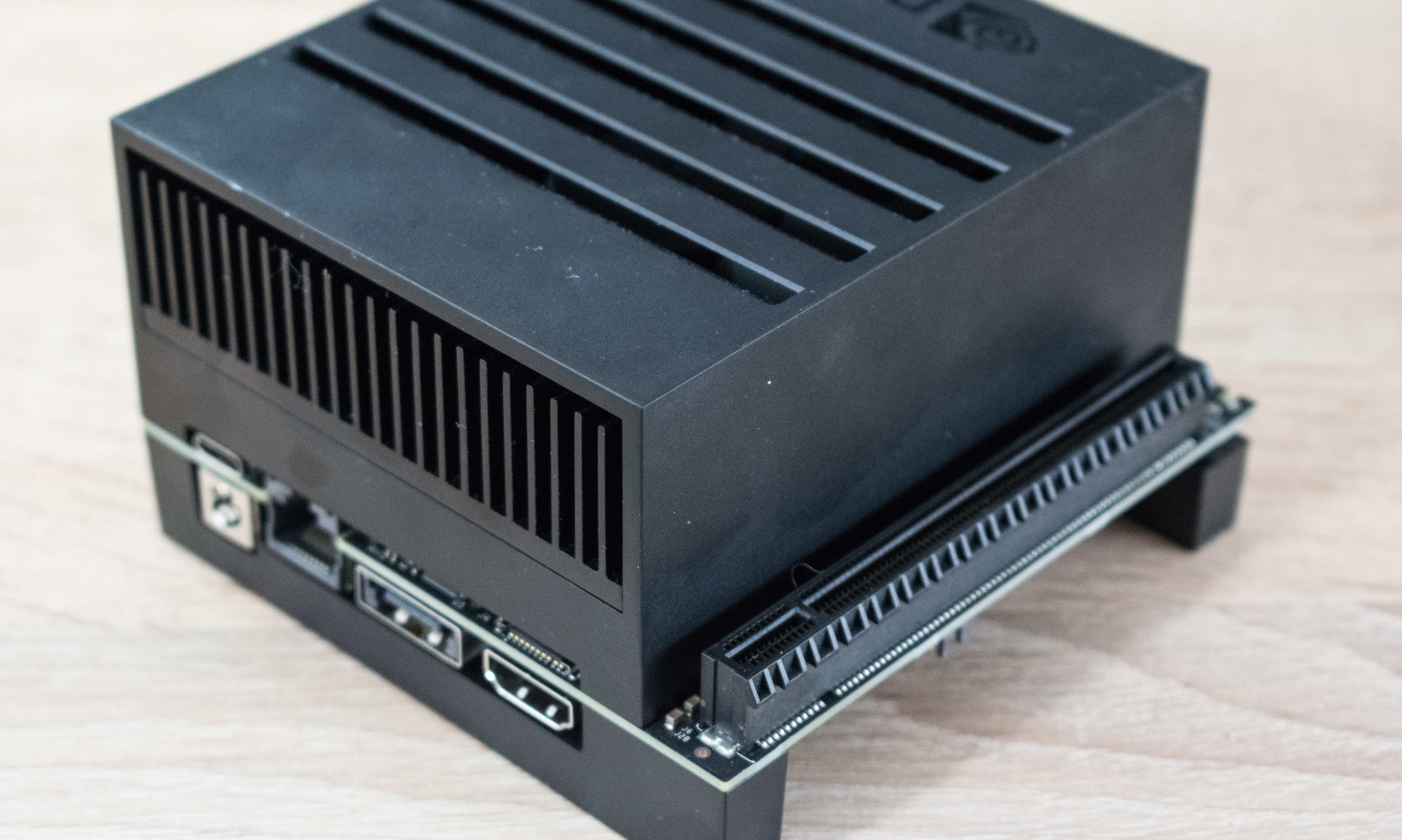
The more unusual connectivity options of the Jetson AGX are the PCIe Gen4 x16 slot as well as a M.2 PCIe x1 extension slot that is meant to be used for connectivity add-ons such as WiFi or cellular modules, both features that aren’t common among Arm development board as most SoCs don’t have the spare PCIe controllers.

The board comes with many other connectors, and that’s one regard in which the new Jetson AGX doesn’t lack at all in flexibility. Power is supplied by an external generic 19V power supply – the stock one supplied by NVIDIA is a 65W LiteOn unit that seems no different than most laptop charger bricks.
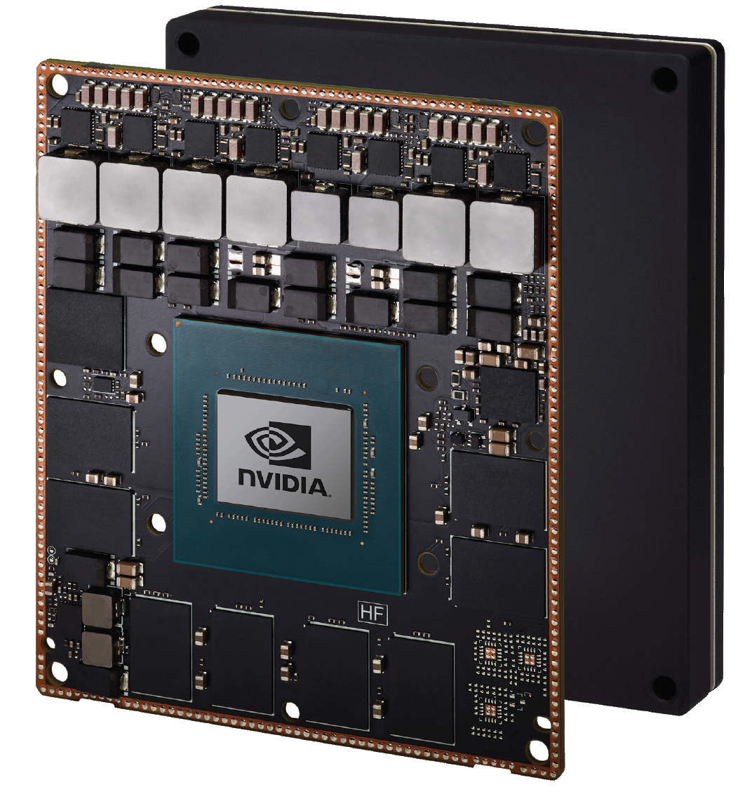
Underneath the quite heavy and solid aluminium heatsink we find what actually powers the Jetson AGX board: the AGX Xavier module. This is a system module that sits on top of the Jetson motherboard – the module has no I/O ports by itself and merely serves as the brains of the system, integrating the core components surrounding the Xavier chip, such as the 16GB of LPDDR4x memory, a small 32GB eMMC storage chip as well as all the power delivery circuits for powering the different power rails of the DRAM as well as IP blocks of the Xavier SoC.
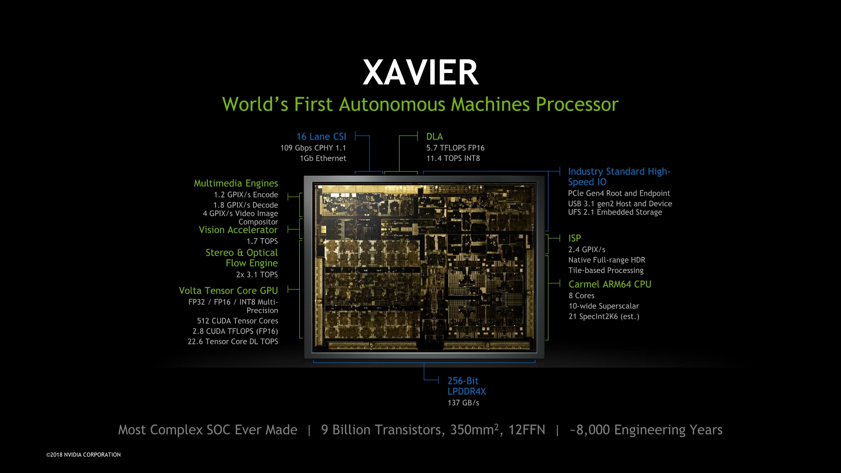
The Xavier chip, as said, is the brains of the platform and represents NVIDIA’s biggest and most complex SoC to date. With 9 billion transistors on a die size of 350mm², it’s among one of the heavyweights of the Arm ecosystem, although between its initial announcements and today Apple has one-upped NVIDIA in terms of transistor count as the new A12X is a 10B chip – in a much smaller manufacturing node.
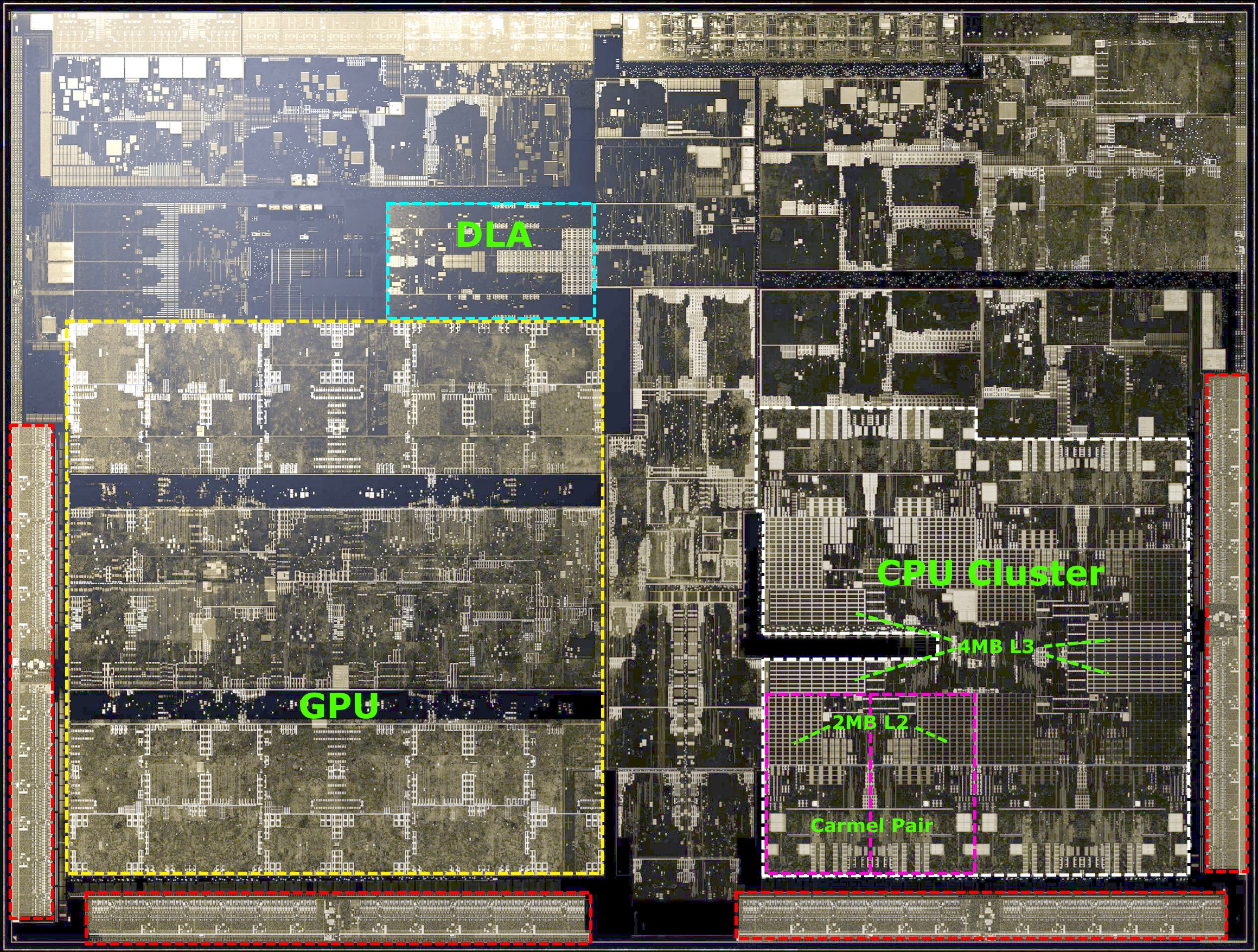
Coming from the traditional PC industry, NVIDIA doesn’t shy away from showing die shots of their products, which is something that is quite rare these days among the Arm SoC vendors. The Xavier SoC is mainly dominated by two big IP blocks which consist of the majority of the space allocated on the die: The 8-core “Carmel” CPU complex as well as a four-cluster Volta GPU.
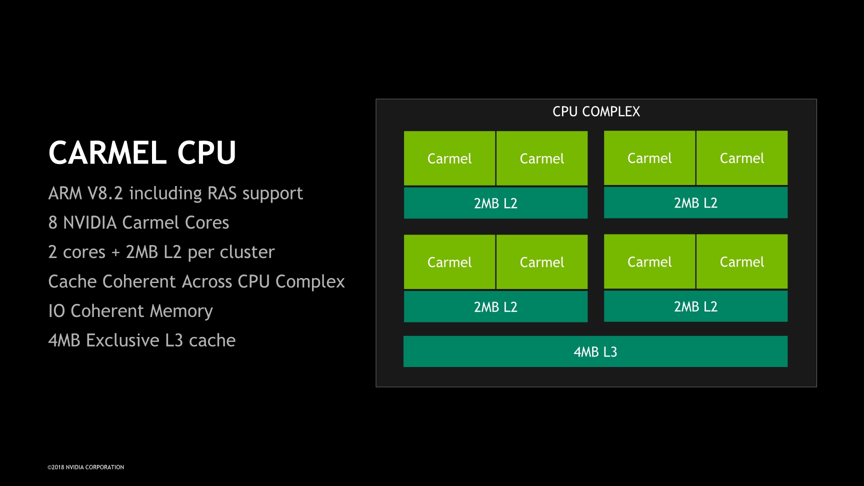
At the high level, the CPU complex contains 8 Carmel CPU cores configured in four clusters, each with a pair of Carmel CPU cores. Each cluster has an independent clock plane and shares a 2MB cache among two CPU cores. At the higher CPU complex level we find a 4MB L3 cache serving all clusters. We don’t know too much about the microarchitecture of the new Carmel cores - seemingly this looks to be a successor to NVIDIA’s Denver µarch, a design that was characterised by its dynamic code optimisation capability. The only thing that NVIDIA does advertise is that this is a 10-wide superscalar machine (10 execution ports in this case, not 10-wide decode) and has support for the ARMv8.2+RAS instruction set. We’ll come back to the CPU core later in the article.
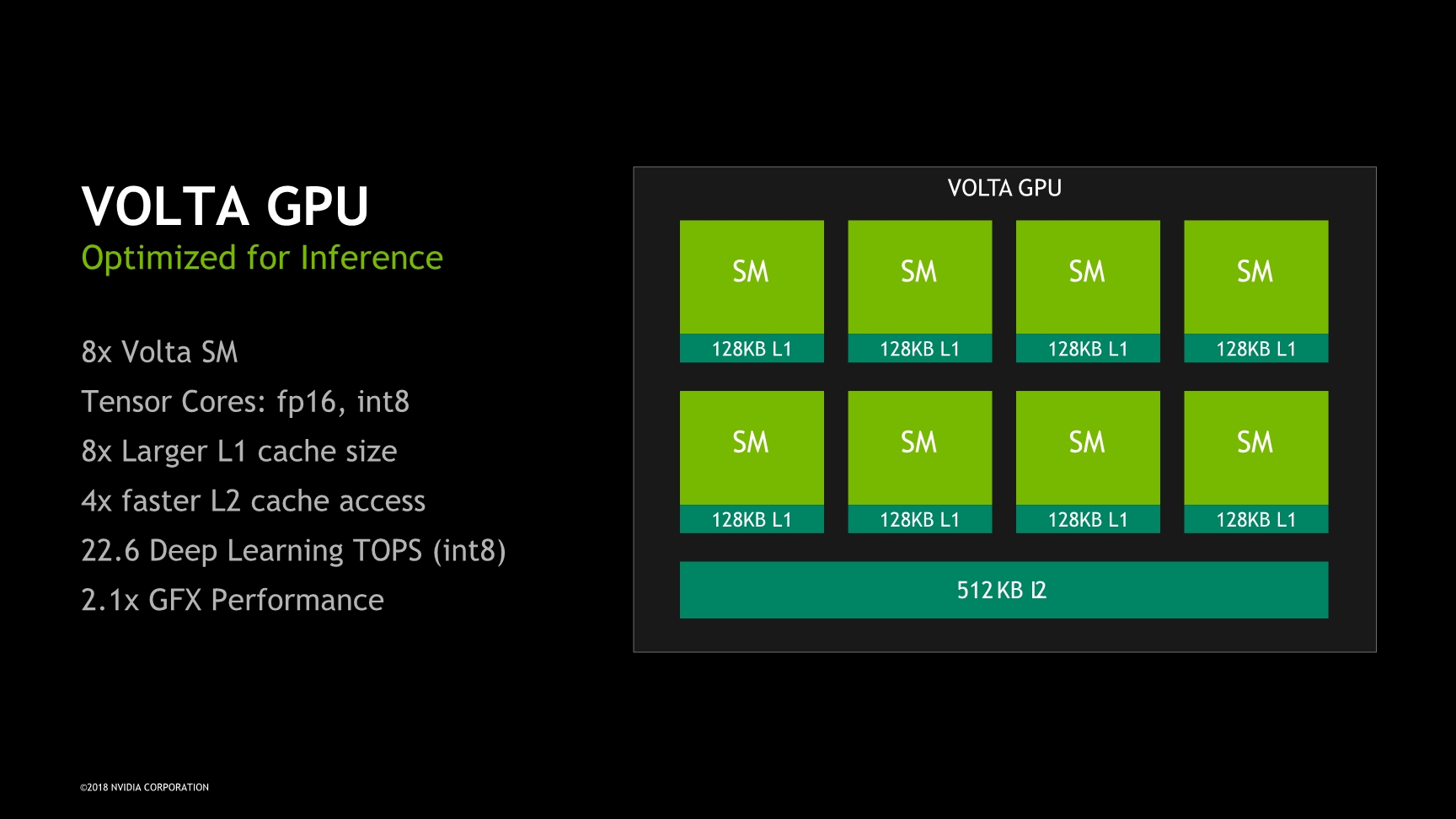
The GPU in Xavier has its roots in the Volta architecture. Here we find the GPU configured into four TPC (Texture processing clusters), each with two SMs (Stream multiprocessors), for a total of 8 SMs or 512 ALU lanes/CUDA cores. A most interesting aspect of the GPU is that because it is based on Volta, it also inherits the Tensor processing units from its bigger brethren. This augments the total processing power of the GPU by up to 22.6 8-bit TOPs or 11.3 FP16 TOPS on the part of the Tensor cores, on top of the respectively 2.8 and 1.4 TFLOPs for FP16 and FP32 CUDA operations provided by the SMs.
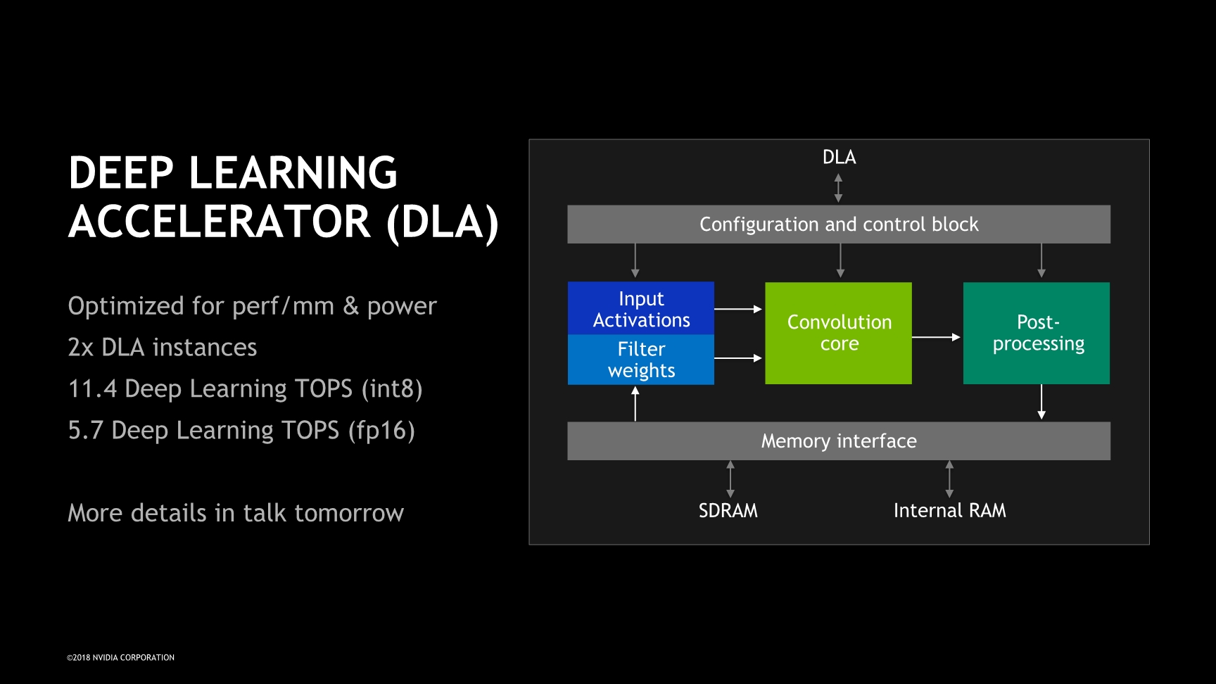
Alongside the CPU and GPU there’s many other important blocks, many of which NVIDIA had covered already at its HotChips 2018 presentation last summer. The one block that really does augment the Xavier SoC is the new DLA IP block: this is very much a new type of block that follows the trend we’ve seen in the mobile SoC space – a dedicated machine inferencing acceleration unit not unlike that which we’ve seen from the likes of HiSilicon or Apple. NVIDIA’s DLA promises performances of up to 11.4 int8 TOPS and is also capable of FP16 operation at half speed at 5.7 TOPS. On the SoC, the unit is implemented as a dual-core instance.

Alongside the DLA, the programmable vision accelerator is again a key component of the Xavier system that allows it focus on vision and in particular robotics, embedded AI and automotive use-cases. The PVA is a more traditional vision IP block that handles more rudimentary tasks such as object detections in a much more efficient way than it would be able to be handled by the GPU or machine inferencing algorithms. Here the PVA will be the first IP block after the ISP in the vision pipeline that will serve to segment parts of an image into objects that will be then forwarded to other algorithms that then would happen on the GPU or DLA.


51 Comments
View All Comments
syxbit - Friday, January 4, 2019 - link
I wish Nvidia hadn't abandoned the mobile space. They could have brought some much needed competition :( :(.Despoiler - Friday, January 4, 2019 - link
The only design that was competitive was the one selected by Google for one generation. 4 ARM cores + a 5th core for power management was a huge failure when everyone can do PM within the ARM SOC. It was only cost competitive in other words.syxbit - Friday, January 4, 2019 - link
The Tegra X1 was a great chip when released.The Shield TV still uses it, and it's an excellent (though now old) chip.
Alistair - Friday, January 4, 2019 - link
And that's not a mobile device. Perf/W for Xavier is also really poor vs. the newest Huawei silicon also.BenSkywalker - Friday, January 4, 2019 - link
The Switch is mobile. When the x1 debuted *four* years ago it obliterated the best from Apple, roughly 50%-100% faster on the gpu side. So yes, if we give the other soc manufacturers four years and a four process step advantage, they can edge out Tegra.Qualcomm's lawyers should take a bow on nVidia not being still present in the mobile market, certainly not the laughable "competition" they had on the technology side.
"Having a hard time seeing a path forward"... That was a cringe worthy line. Why not benchmark direct x on an iPhone and then say the same about the Ax line? Let's take a deep learning/ai platform and benchmark it using antiquated pc desktop applications and then act like there are fundamental design issues... ?
TheinsanegamerN - Friday, January 4, 2019 - link
The tegra X1 doesnt run anywhere near full speed when the device is not plugged into a power source. The Switch also has a fan. It's pretty easy to "obliterate" the competition when you are using a different form factor. I mean, the core I7 with iris pro 580 GPU obliterates the tegra X1, so the X1 must not be very good right?The X1 was WAY too power hungry to use in anything other then a dedicated gaming device with a dedicated cooling system. When restricted down to tablet TDPs, the X1's performance drops like a lead rock.
So, yeah, maybe with another 4 years nvidia could make the tegra work in a proper laptop. Meanwhile, Apple has ALREADY done that with the A12 SoC, and that works in a passive tablet. Nvidia was never able to make their SoC work in a similar system.
Alistair - Saturday, January 5, 2019 - link
Are you replying to my comment? Xavier is new for 2018 and so is Huawei's Kirin 980. We are talking about Xavier, not X1. And Apple's tablet GPU for 2015 equaled nVidia's in perf. The iPad Pro's A9X equalled the Tegra x1 in GPU performance while surpassing it in CPU performance, and at a lower power draw...Alistair - Saturday, January 5, 2019 - link
I think you were conveniently comparing the 2014 iPad's vs. the 2015 X1, instead of the 2015 iPad Pro vs. the X1.Samus - Saturday, January 5, 2019 - link
^^thisniva - Friday, January 4, 2019 - link
Why are there video ads automatically playing on each one of the Anandtech pages? I know you guys are trying to monetize but you've crossed lines that make it annoying for your users to keep visiting the site.