HBM4

Under the CHIPS & Science Act, the U.S. government provided tens of billions of dollars in grants and loans to the world's leading maker of chips, such as Intel, Samsung, and TSMC, which will significantly expand the country's semiconductor production industry in the coming years. However, most chips are typically tested, assembled, and packaged in Asia, which has left the American supply chain incomplete. Addressing this last gap in the government's domestic chip production plans, these past couple of weeks the U.S. government signed memorandums of understanding worth about $1.5 billion with Amkor and SK hynix to support their efforts to build chip packaging facilities in the U.S. Amkor to Build Advanced Packaging Facility with Apple in Mind Amkor plans to build a $2 billion advanced...

TSMC Readies Next-Gen HBM4 Base Dies, Built on 12nm and 5nm Nodes
Of the several major changes coming with HBM4 memory, one of the most immediate is the sheer width of the memory interface. With the fourth-generation memory standard moving from...
1 by Anton Shilov on 5/16/2024
SK hynix to Build $3.87 Billion Memory Packaging Fab in the U.S. for HBM4 and Beyond
SK hynix this week announced plans to build its advanced memory packaging facility in West Lafayette, Indiana. The move can be considered as a milestone both for the memory...
7 by Anton Shilov on 4/5/2024
Report: SK Hynix Mulls Building $4 Billion Advanced Packaging Facility in Indiana
SK hynix is considering whether to build an advanced packaging facility in Indiana, reports the Wall Street Journal. If the company proceeds with the plan, it intends to invest...
4 by Anton Shilov on 3/26/2024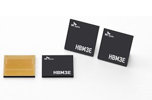
SK Hynix Mulls 'Differentiated' HBM Memory Amid AI Frenzy
SK Hynix and AMD were at the forefront of the memory industry with the first generation of high bandwidth memory (HBM) back in 2013 – 2015, and SK Hynix...
10 by Anton Shilov on 3/1/2024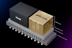
HBM4 in Development, Organizers Eyeing Even Wider 2048-Bit Interface
High-bandwidth memory has been around for about a decade, and throughout its its continued development it has steadily increased in speed, starting at a data transfer rate from 1...
11 by Anton Shilov on 10/12/2023
Micron Publishes Updated DRAM Roadmap: 32 Gb DDR5 DRAMs, GDDR7, HBMNext
In addition to unveiling its first HBM3 memory products yesterday, Micron also published a fresh DRAM roadmap for its AI customers for the coming years. Being one of the...
4 by Anton Shilov on 7/27/2023
Micron Announces 20-Year Plan To Build $100 Billion U.S. Fab Complex
Now that the U.S. government has finally settled the matter of whether it would be providing subsidies to entice chip fabs to setup shop within the U.S., those fabs...
48 by Anton Shilov on 10/10/2022


