ELSA GLADIAC ULTRA 64MB GeForce2 Ultra
by Anand Lal Shimpi on October 12, 2000 2:47 AM EST- Posted in
- GPUs
The Card
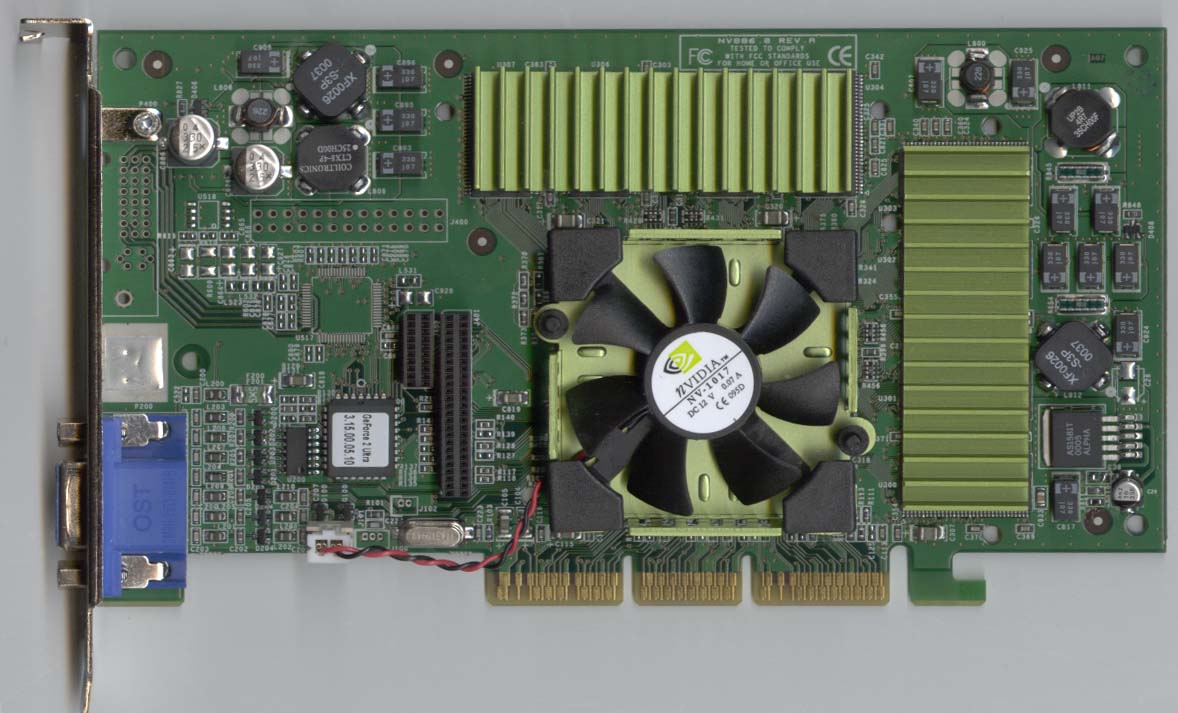
Just as with the GeForce2 GTS based GLADIAC, ELSA didn’t stray far from NVIDIA’s reference design with their GLADIAC ULTRA. Unlike in the early days of graphics cards, reference designs are now the way to go for manufacturers like ELSA, since they are designed very well and are extremely easy to implement. In contrast, just a few years ago, the same could definitely not be said about the kings of the graphics industry back then and their reference designs.
Needless to say, by adhering to NVIDIA’s reference design, ELSA not only cuts down on development time for the card, but they can also put it on shelves much quicker than they would be able to if they had come up with their own design. This is obviously a sacrifice they make as the reference design has no room for added features such as the multitude of video input and output ports we see on ASUS’ Deluxe series of GeForce and GeForce2 GTS based cards. ELSA does take a unique approach to tackling this tradeoff, which we will discuss later on.
As with all Ultra based boards, the GLADIAC ULTRA features the 0.18-micron GeForce2 Ultra core which runs at 250MHz. As we concluded in our review of the GeForce2 Ultra, these Ultra chips are essentially hand picked GeForce2 GTS cores that happen to hit the higher clock speed specified by NVIDIA, much like how the TNT2 Ultra chips were distinguished from the regular TNT2 chips during their reign.
ELSA GLADIAC
ULTRA
GeForce2
Ultra Reference Design
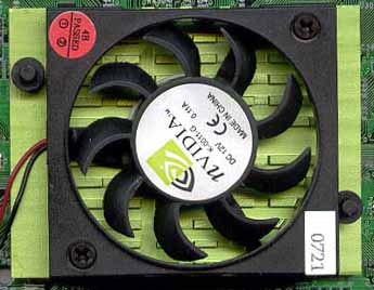
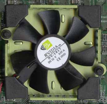
In cooling this high clocked core, ELSA implemented an even larger heatsink/fan combo than what we saw on the reference Ultra board we received from NVIDIA in August. The heatsink measures 2” x 2” (5.08 cm x 5.08 cm), while the reference design heatsink was approximately 2.25” x 1.75”. The resulting surface area of the heatsink on the GLADIAC ULTRA is about 2% larger than what was present on the reference board, but that alone shouldn’t provide for a dramatic increase in cooling efficiency.
However, ELSA has also implemented a larger fan to go along with this larger heatsink. Instead of the 10 finned fan that spanned a diameter of 1.5” as we noticed on the reference board, ELSA implemented a fan with 7 larger fins and a full 2” diameter to aid in cooling the Ultra’s core. The two fans appear to spin at the same rate, meaning that ELSA’s fan should be effectively a better cooler than what we saw on the reference boards.
ELSA implements the same two heatsinks that we saw on the reference board across its 8 ESMT SDRAM chips. These SDRAM chips are rated at 4ns, giving them a theoretical maximum operating frequency of 250MHz DDR (effectively 500MHz). With the GLADIAC ULTRA, as well as all other Ultra based boards, shipping with a 460MHz effective memory clock, this opens up quite an avenue for overclockers to experiment with. NVIDIA’s reason for specifying a 460MHz memory clock while using 500MHz SDRAM is simple, the yields on these 4ns parts aren’t high enough to allow for them to successfully operate at 500MHz on an Ultra board 100% of the time. Thus by rating the GeForce2 Ultra’s memory clock at 460MHz NVIDIA is essentially playing it safe, however for those that don’t mind playing in the realm of overclocked frequencies, the chances of hitting 500MHz are pretty good.
Unlike the ‘RAMsinks’ we saw on Guillemot’s (Hercules) 3D Prophet II GTS which didn’t really do much at all, the heatsinks on the GLADIAC ULTRA actually do help cool those extremely hot running memory chips. As we found in our GeForce2 Ultra review, removing just one of the two heatsinks compromised stability.


0 Comments
View All Comments