Analyzing Intel-Micron 3D XPoint: The Next Generation Non-Volatile Memory
by Kristian Vättö, Ian Cutress & Ryan Smith on July 31, 2015 11:00 AM EST
The current mainstream memory technologies, namely DRAM (quick memory accessed by the processor) and NAND (solid-state storage), have been around for decades. While the cell designs have evolved over the years to allow scaling to 20nm and below, the fundamental physics behind DRAM and NAND operation haven't changed a bit and both technologies have their unique technological limitations. DRAM offers nanosecond-level latency and unlimited endurance, but this comes at the cost of large cell size, cell volatility, and power consumption. Since DRAM cells need to be constantly refreshed, the cells don't retain data in an off state, requiring quite a bit of power and making DRAM unsuitable for permanent storage. NAND, on the other hand, has much higher latency (especially write operations) and has a limited number of write cycles, but the cells are non-volatile and the structure is much more efficient, enabling low cost and suitability for storage.
Combining DRAM and NAND at the system-level architecture provides the best of both worlds, which is why modern computers use DRAM as a memory/cache and NAND for storage. However, there's still a latency and capacity gap between DRAM and NAND, so the question arises: what if you were to combine the best of DRAM and NAND at the silicon level? The mission of next generation memory technology across the industry has been to develop a new type of memory that provides low latency and high endurance while offering a small and scalable cell size.
We have seen numerous startups, such as Crossbar and Nantero, discuss and demonstrate their next generation memory technologies, but we have yet to see the established DRAM and NAND vendors come out with their solutions. Intel and Micron are here to change that with the announcement of their new 3D XPoint (Cross Point) non-volatile memory technology this week.
First and foremost, Intel and Micron are making it clear that they are not positioning 3D XPoint as a replacement technology for either NAND or DRAM, and in that scale it has been talked about more in its applications nearer NAND than DRAM. It's supposed to complement both and provide a technology that sits in between the two by filling the latency and cost gap exists between DRAM and NAND. Basically, 3D XPoint is a new tier in the computer architecture because it can be used as either slower, non-volitile memory or much faster storage.
| DRAM | 3D XPoint | NAND | |
| Endurance (P/E Cycles) | 10^15 | 10^7 | 10^3 |
| Read Latency | Nanoseconds | 10s of Nanoseconds | ~100 Microseconds |
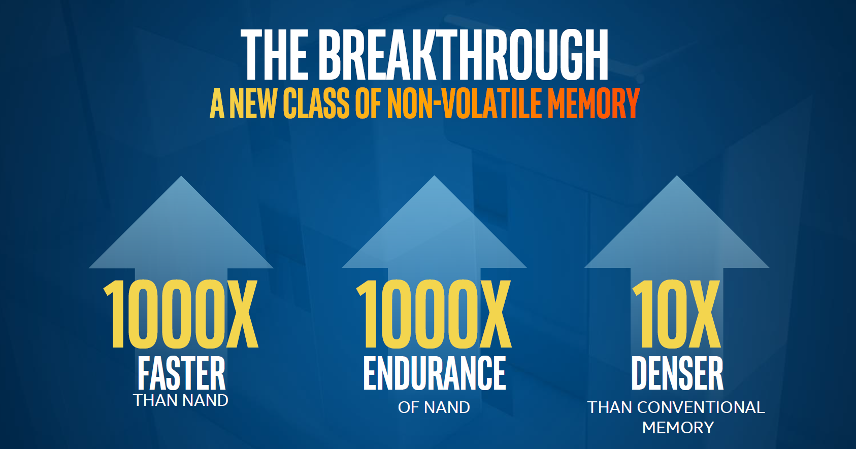
Intel and Micron are claiming that 3D XPoint provides up to a thousand times higher endurance than NAND. Assuming that the numbers are relative to modern (15-20nm) MLC NAND, the endurance should be in the order of a few million P/E cycles; though the marketing materials are claiming up to tens of millions of write cycles. If we assume 3 million write cycles (1000x of what modern MLC has), a 256GB 3D XPoint based drive would have a total write endurance of 768 petabytes. That's equivalent to 420TB per day for five years, or 4.9GB per second. For storage applications that currently rely on NAND, 3D XPoint will eliminate any potential endurance concerns, but it's not durable enough to challenge DRAM in that front since DRAM endurance is essentially infinite. Whether 3D XPoint provides enough endurance to replace DRAM ultimately depends on the application, but especially in certain enterprise workloads there's a need for DRAM.
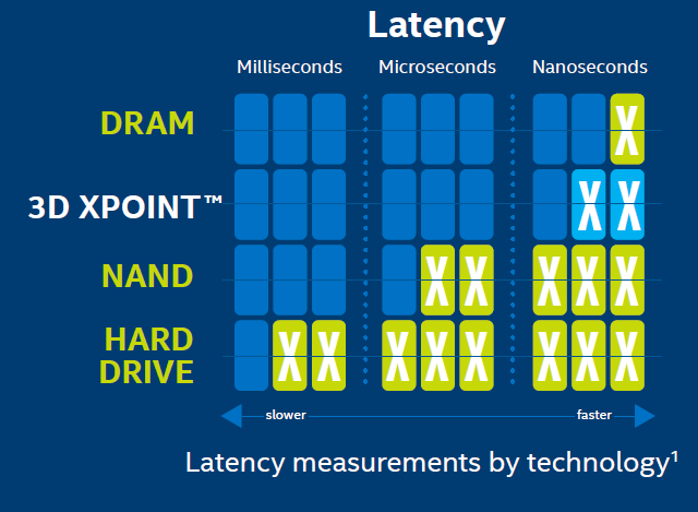
3D XPoint latency should be in the order of 10s of nanoseconds, but the companies didn't specify whether this is read or write latency. Judging by the graphs provided by Intel, it seems to be read latency because NAND write latency would measured in milliseconds (typically 1-2ms for a full page write), whereas the graph puts NAND latency at tens of microseconds that is in line with NAND read latency. Write latency is likely higher than that, probably at least 100s of nanoseconds or even a few microseconds given Intel and Micron's claims of "up to 1000x faster than NAND", but what complicates things is that 3D XPoint is accessible at the bit-level whereas NAND is page-level, so comparing the latency of the two without extended context is quite difficult. In any case, 3D XPoint performance should be closer to DRAM than NAND, but since Intel and Micron aren't discussing any specific latencies yet it's too early to make any final conclusions.
Meanwhile unlike many next generation memory technologies out there at the moment, 3D XPoint is the furthest along and doesn't only exist on paper or in a lab. Intel and Micron are currently sampling the first generation die that is being produced at the companies' jointly owned fab in Lehi, Utah. The die is 128Gbit (16GB) in capacity, whereas the products that startup memory companies have in production are in the order of dozens of megabytes. The die is built on a 20nm node and consists of two layers, and in the future scaling will happen through both lithography shrinks and by increasing the number of layers.
The Utah fab has been producing 20nm NAND for now since Intel didn't invest on the 16nm shrink and all initial 3D NAND production will take place in Micron's Singapore fab, but it's unclear whether the full fab with its 20,000 wafers per month capacity will be dedicated to 3D XPoint from now on. My guess would be that 3D XPoint will gradually take over the full wafer capacity in Utah depending on how the market reacts to the new technology and how high demand Intel and Micron are seeing. 3D XPoint does require some new equipment for manufacturing since 3D XPoint deals with a whole new set of materials, but Intel and Micron said that the transition is quite similar to a new NAND node and allows some of the existing equipment to be used.
The companies aren't quoting any price per gigabyte yet, but since the whole function of 3D XPoint is to fill the gap between DRAM and NAND, it will also be priced accordingly. A quick look at NewEgg puts DRAM pricing at approximately $5-6 per gigabyte, whereas the high-end enterprise SSDs are in the range of $2-3. While client SSDs can be had for as low as $0.35, they aren't really a fair comparison because at least initially 3D XPoint will be aimed for enterprise applications. My educated guess is that the first 3D XPoint based products will be priced at about $4 per gigabyte, possibly even slightly lower depending on how DRAM and NAND pricess fall within a year.


80 Comments
View All Comments
Ian Cutress - Saturday, August 1, 2015 - link
Most likely they're wanting to protect their investment and not let the cat out of the bag for others to copy. Keeping IP close to the chest and industry secrets is part of the game is important, especially if there's 10 years of funding behind it. That's why we don't get any insights at all into things like Qualcomm's Adreno graphics and such - to them they want us to consider it a black box and that's all they're willing to speak on the issue.There may be something legal too. Can't discount that for sure.
jjj - Saturday, August 1, 2015 - link
Don't confuse the public with the competition. Why they hide from the public, ask their IR and marketing.Their competitors know a lot more and a lot sooner than you imagine. When corporations claim"competitive reasons" it's a flat out lie 99.99% of the time. Here once they start sampling there is nothing to hide anymore and they'll do that soon enough although there have been rumors about the tech and some might be working on controllers for the thing already so the relevant competitors might have all the info they need- Samsung has been involved in plenty of scandals over the year, Toshiba is in the middle of one right now so don't imagine for a minute that big corporations have any kind of ethics and they won't do what they need to do to obtain info.Micron has it's summer analyst day on August 14 and they will disclose more then, remains to be seen how much.
Tunnah - Saturday, August 1, 2015 - link
This post literally gave me a headache.Damn I wish I was smarter. Although from what I could...grasp (and I use that term so incredibly loosely) it looks awesome.
One question I had though, if it's faster by a large margin than NAND, and more reliable, does that mean the introductory pricing will push enterprise SSD costs down, or simply be artificially inflated as to not damage the profit margins from that sector ?
Ian Cutress - Saturday, August 1, 2015 - link
It's difficult to say at this point as it depends on what product segment will exploit XPoint the most. If we're looking at an intermediary for database applications, it might need a change on the hardware level and certainly at a software level, and be sold different to storage. If it's acting as an SSD replacement, you'll most likely see it being sold at a premium against 3D NAND technologies and the market will adjust accordingly. There's also the aspect of competition too, and if anyone else will have something in this space soon.Kristian Vättö - Monday, August 3, 2015 - link
Just to add to Ian's comment, there was also a private "Meet the Architect" Q&A after the webinar with Micron's VP of R&D and one of Intel's Senior Fellows and the two went into great detail of how PCM never ended up being viable to replace DRAM due to scaling issues.witeken - Friday, July 31, 2015 - link
How about PCMS? This very informed article a number of weeks ago predicted it would be PCMS. He makes a very strong case, and that was before the announcement.http://seekingalpha.com/article/3253655-intel-and-...
name99 - Friday, July 31, 2015 - link
Obsessing about this is idiotic.Intel/Micron is avoiding certain language because that language has an unfortunate past (cf Windows Vista becomes Windows 7 --- "is it Windows Vista? No no no, Completely new OS"...)
Whether it's phase change or not (or whether changing the material from one state to another counts as a phase change) is utterly irrelevant to anyone except the manufacturer. It's like if Intel announced 3D-NAND and the question everyone felt worth asking was what color the masks are.
The questions that DO matter are the user-facing questions --- performance (read and write), power, cost, reliability, form factor.
Ian Cutress - Saturday, August 1, 2015 - link
As an end-user, yes it doesn't ultimately matter what the underlying technology is.As an analyst interested in the science behind the industry, or if you were a financial investment agent looking into the market to see which technologies are keeping which companies in growth figures with potential market share adjustments, it's an absolute must-know.
User facing questions are about how the product is used. Business facing questions are about how the product fits in, and the technology behind it. Research related questions are about exploiting fundamental laws of physics in different ways, regardless of the name. All of these questions matter, even if you're not involved in the latter two segments.
Refuge - Monday, August 3, 2015 - link
This is Anandtech right? I didn't click on the wrong link?I thought this site existed solely because we all obsess over the latest tech, and appreciate knowing how the nitty gritty's all work together. ;)
KateH - Friday, July 31, 2015 - link
This seems like it would compliment HBM well. If an APU was made with "only" 4-8GB of on-package memory, but could use swap space on a XPoint partition, the performance hit from paging could be pretty minor.