Intel SSD 750 PCIe SSD Review: NVMe for the Client
by Kristian Vättö on April 2, 2015 12:00 PM EST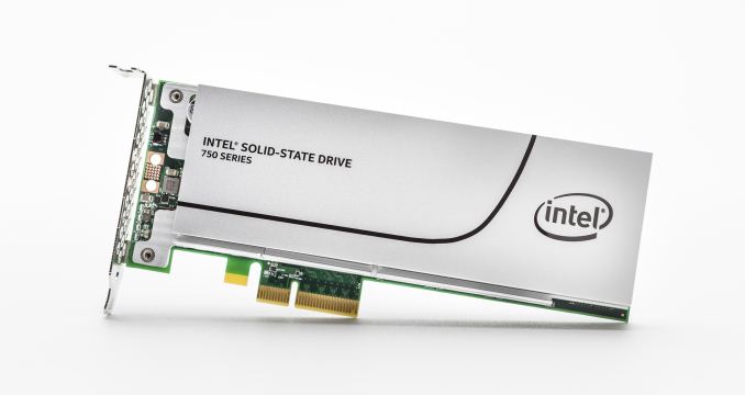
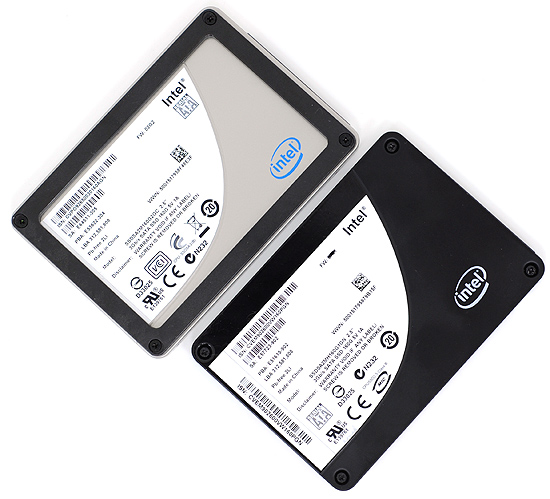
I don't think it's an overstatement to say that Intel introduced us to the era of modern SSDs back in 2008 with the X25-M. It wasn't the first SSD on the market, but it was the first drive that delivered the aspects we now take for granted: high, consistent and reliable performance. Many SSDs in the early days focused solely on sequential performance as that was a common performance metric for hard drives, but Intel understood that the key to better user performance wasn't the maximum throughput, but the small random IOs that take unbearably long to complete on HDDs. Thanks to Intel's early understanding of real world workloads and implementing the knowledge to a well designed product, it took several years before others were able to fully catch up with the X25-M.
But when the time came to upgrade to SATA 6Gbps, Intel missed the train. The initial SATA 6Gbps drives had to rely on third party silicon because Intel's own SATA 6Gbps controller was still in development, and to put it frankly the SSD 510 and SSD 520 just didn't pack the same punch as the X25-M did. The others had also done their homework and gone back to drawing board, which meant that Intel was no longer in the special position it was in 2008. Once the SSD DC S3700 with in-house Intel SATA 6Gbps controller finally materialized in late 2012, it quickly built back the Intel image that the company had in the X25-M days. The DC S3700 wasn't as revolutionary as the X25-M was, but it again focused on areas where other manufacturers had been lacking, namely performance consistency.
The first and second generation Intel X25-M
While Intel was arguably late to the SATA 6Gbps game, the company already had something much bigger in its mind. Something that would abandon the bottlenecks of SATA interface and challenge the X25-M in significance in the history of SSDs. That product was the SSD DC P3700, the world's first drive with custom PCIe NVMe controller and the first NVMe drive that was widely available.
Ever since our SSD DC P3700 review, there's been massive interest from enthusiasts and professionals for a more client-oriented product based on the same platform. With eMLC, ten drive writes per day endurance and a full enterprise-class feature set, the SSD DC P3700 was simply out of reach for consumers at $3 per gigabyte because the smallest 400GB SKU cost the same as a decent high power PC build. Intel didn't ignore your prayers and wishes and with today's release of the SSD 750 Intel is delivering what many of you have been craving for months: NVMe with a consumer friendly price tag in a 2.5" form factor via SFF-8639 or a PCIe add-in card.
| Intel SSD 750 Specifications | |||
| Capacity | 400GB | 1.2TB | |
| Form Factor | 2.5" 15mm SFF-8639 or PCIe Add-In Card (HHHL) | ||
| Interface | PCIe 3.0 x4 - NVMe | ||
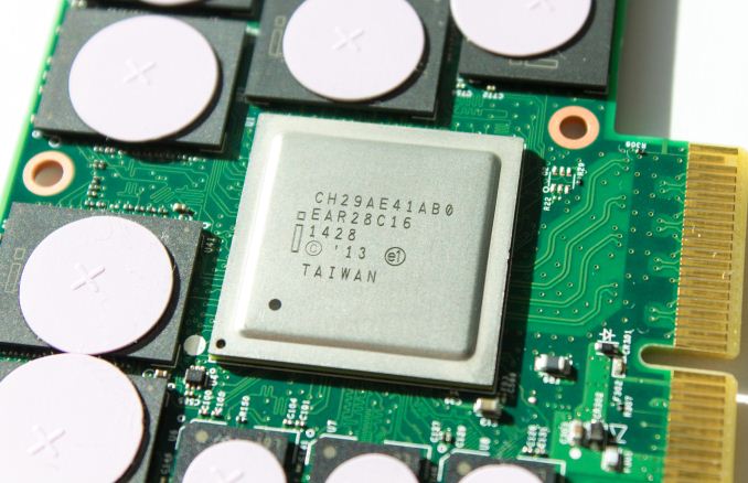
| Controller | Intel CH29AE41AB0 | ||
| NAND | Intel 20nm 128Gbit MLC | ||
| Sequential Read | 2,200MB/s | 2,400MB/s | |
| Sequential Write | 900MB/s | 1,200MB/s | |
| 4KB Random Read | 430K IOPS | 440K IOPS | |
| 4KB Random Write | 230K IOPS | 290K IOPS | |
| Idle Power Consumption | 4W | 4W | |
| Read/Write Power Consumption | 9W / 12W | 10W / 22W | |
| Encryption | N/A | ||
| Endurance | 70GB Writes per Day for Five Years | ||
| Warranty | Five Years | ||
| MSRP | $389 | $1,029 | |
Even though the SSD 750 is built upon the SSD DC P3700 platform, it's a completely different product. Intel spent a lot of time on redesigning the firmware to be more suitable for client applications, which differ greatly from typical enterprise workloads. The SSD 750 is supposed to be more focused on random performance as the majority of IOs in client workloads tend to have random patterns and be small in size. The sequential write speeds may seem a bit low for such high capacities for that reason, but ultimately Intel's goal was to provide better real world performance rather than focus on maximum benchmark numbers, which has been Intel's strategy ever since the X25-M days.
At the time of launch, the SSD 750 will only be available in capacities of 400GB and 1.2TB. An 800GB SKU is being considered, but I think Intel is still testing the waters with the SSD 750 and thus the initial lineup is limited to just two SKUs. After all, the ultra high-end is a niche market and even in that space the SSD 750 is much more expensive that existing SATA drives, so a gradual roll out makes a lot of sense. I think for enthusiasts the 400GB model is the sweet spot because it provides enough capacity for the OS and applications/games, whereas professionals will likely want to spring for the 1.2TB if they are looking for high-speed storage for work files (video editing is a prime example).
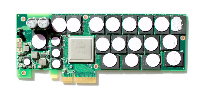
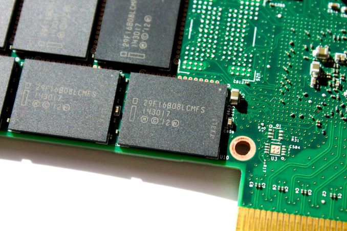
The SSD 750 utilizes Intel-Micron's 20nm 128Gbit MLC NAND. The die configuration is actually fairly interesting because the packages on the front-side on the PCB (i.e. the one that's covered by the heat sink and where the controller is) are quad-die with 64GiB capacity (4x128Gbit), whereas the packages on the back-side of the PCB are all single-die. I suspect Intel did this for heat reasons because PCIe is more capable of utilizing NAND to its full potential, which increases the heat output and obviously four dies inside one package generate more heat than a single die. With 18 packages on the front-side and 14 on the backside, the raw NAND capacity comes in at 1,376GiB, resulting in effective over-provisioning of 18.8% with 1,200GB of usable capacity.
The controller is the same 18-channel behemoth running at 400MHz that is found inside the SSD DC P3700. Nearly all client-grade controllers today are 8-channel designs, so with over twice the number of channels Intel has a clear NAND bandwidth advantage over the more client-oriented designs. That said, the controller is also much more power hungry and the 1.2TB SSD 750 consumes over 20W under load, so you won't be seeing an M.2 variant with this controller.
Similar to the SSD DC P3700, the SSD 750 features full power loss protection that protects all data in the DRAM, including user data in flight. I'm happy to see that Intel understands how power loss protection can be a critical feature for the high-end client segment as well because especially professional users can't have the risk of losing any data.
The Form Factors & SFF-8639 Connector
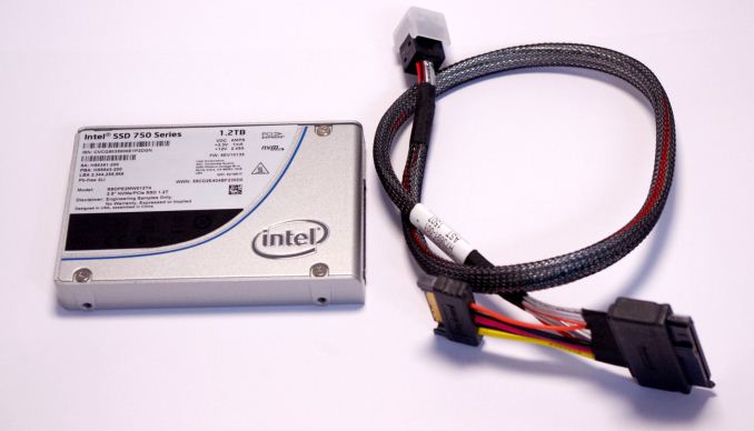
The SSD 750 is available in two form factors: a traditional half-height, half-length add-in card and 2.5" 15mm drive. The 2.5" form factor utilizes an SFF-8639 connector that is mostly used in the enterprise, but it's slowly making its way to the high-end client side as well (ASUS just announced TUF Sabertooth X99 two weeks ago at CeBit). The SFF-8639 is essentially SATA Express on steroids and offers four lanes of PCIe connectivity for up to 4GB/s of bandwidth with PCIe 3.0 (although in real world the maximum bandwidth is about 3.2GB/s due to PCIe inefficiency). Honestly, aside from the awkward name, SFF-8639 is what SATA Express should have been from the beginning because nearly all upcoming PCIe controller designs will feature four PCIe lanes, which renders SATA Express useless as there's no point in handicapping a drive with an interface that's only capable of providing half of the available bandwidth. That said, I wasn't at the table when SATA-IO made the decision, but it's clear that the spec wasn't fully thought through.
The SFF-8639 connector
Similar to SATA Express, SFF-8639 has a separate SATA power input in the cable. That's admittedly quite unwieldy, but it's necessary to keep the motherboard and cable costs reasonable. The SSD 750 requires both 3.3V and 12V rails for power, so if the drive was to draw power from PCIe it would have required some additional components on the motherboard side, which is something that the motherboard OEMs are hesitant about due to the added cost, especially since it's just one port that may not even be used by the end-user.
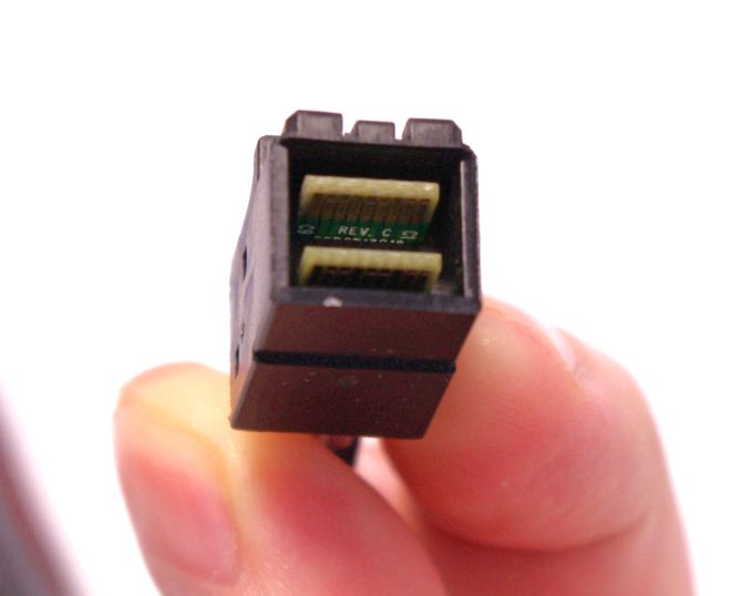
The motherboard end of the SFF-8639 cable
As the industry moves forward and PCIe becomes more common, I think we'll see SFF-8639 being adopted more widely. The 2.5" form factor is really the best for a desktop system because the drive location is not fixed to one spot on the motherboard or in the case. While M.2 and add-in cards provide a cleaner look thanks to the lack of cables, they both eat precious motherboard area that could be used for something else. That's the reason why motherboards don't usually have more than one M.2 slot as the area taken by the slot can't really be used for any other components. Another issue especially with add-in cards is the heat coming from other PCIe cards (namely high power GPUs) that can potentially throttle the drive, whereas drive bays tend to be located in the front of the case with good airflow and no heat coming from surrounding components.
Utilizing the Full Potential of NVMe
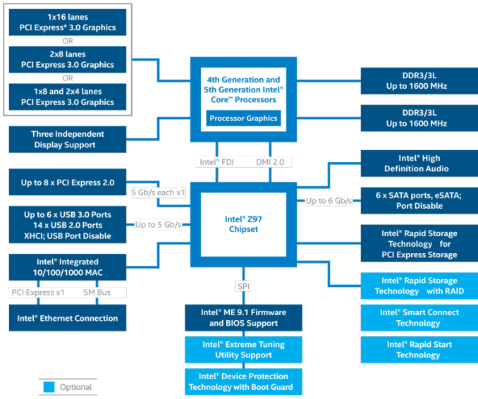
Because the SSD 750 is a PCIe 3.0 design, it must be connected directly to the CPU's PCIe 3.0 lanes for maximum throughout. All the chipsets in Intel's current line up are of the slower PCIe 2.0 flavor, which would effectively cut the maximum throughput to half of what the SSD 750 is capable of. The even bigger issue is that the DMI 2.0 interface that connects the platform controller hub (PCH) to the CPU is only four lanes wide (i.e. up to 2GB/s), so if you connect the SSD 750 to the PCH's PCIe lanes and access other devices connected to the PCB (e.g. USB, SATA or LAN) at the same time the performance would be even further handicapped.
Intel Z97 chipset block diagram
Utilizing the CPU's PCIe lanes presents some possible bottlenecks for the users of Z97 chipset because the normal Haswell CPUs feature only sixteen PCIe 3.0 lanes. In other words, if you wish to use the SSD 750 with a Z97 chipset you have to give up some GPU PCIe bandwidth because the SSD 750 will take four lanes out of the sixteen. With a single GPU setup that's hardly an issue, but with SLI/CrossFire setup there's a possibility of some bandwidth handicapping if the GPUs and SSD are utilizing the interface simultaneously. Also, with NVIDIA's PCIe x8 requirement, it limits itself to a single NVIDIA card implementation. Fortunately it's quite rare that an application would tax the GPUs and storage at the same time since games tend to load data to RAM for faster access and especially with the help of PCIe switches it's possible to grant all devices the lanes they require (although the maximum bandwidth isn't increased, but switches allow full x16 bandwidth to the GPUs when they need it).
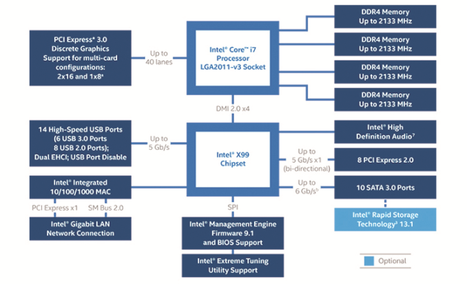
Intel X99 chipset block diagram
With Haswell-E and its 40 PCIe 3.0 lanes, there are obviously no issues with bandwidth even with an SLI/CrossFire setup and two SSD 750s. Unfortunately the X99 (or any other chipset) doesn't support PCIe RAID, so if you were to put two SSD 750s in RAID 0 the only option would be to use software RAID. That in turn will render the volume unbootable and I had some performance issues with two Samsung XP941s in software RAID, so at this point I would advice against RAIDing the SSD 750s. We'll have to wait for Intel's next generation chipsets to get proper RAID support for PCIe SSDs.
As for older chipsets, Intel isn't guaranteeing compatibility with 8-series chipsets and older. The main issue here is that the motherboard OEMs aren't usually willing to support older chipsets in the form of BIOS updates and the SSD 750 (and NVMe in general) requires some BIOS modifications in order to be bootable. That said, some older motherboards may work with the SSD 750 just fine, but I suggest you do some research online or contact the motherboard manufacturer before pulling the trigger on the SSD 750.
Bootable? Yes
Understandably the big question many of you have is whether the SSD 750 can be used as a boot drive. I've confirmed that the drive is bootable in my testbed with ASUS Z97 Deluxe motherboard with the latest BIOS and it should be bootable on any motherboard with proper NVMe support. Intel will have a list of supported motherboards on the SSD 750 product page, which are all X99 and Z97 based at the moment but the support will likely expand over time (it's up to the motherboard manufacturers to release a BIOS version with NVMe support).
Furthermore, I know many of you want to see some actual real world tests that compare NVMe to SATA drives and I'm working on a basic test suite to cover that. Unfortunately, I didn't have the time to include it in this review due to this and last weeks' NDAs, but I will publish it as a separate article as soon as it's done. If there are any specific tests that you would like to see, feel free to make suggestions in the comments below and I'll see what I can do.
| AnandTech 2015 SSD Test System | |
| CPU | Intel Core i7-4770K running at 3.5GHz (Turbo & EIST enabled, C-states disabled) |
| Motherboard | ASUS Z97 Deluxe (BIOS 2205) |
| Chipset | Intel Z97 |
| Chipset Drivers | Intel 10.0.24+ Intel RST 13.2.4.1000 |
| Memory | Corsair Vengeance DDR3-1866 2x8GB (9-10-9-27 2T) |
| Graphics | Intel HD Graphics 4600 |
| Graphics Drivers | 15.33.8.64.3345 |
| Desktop Resolution | 1920 x 1080 |
| OS | Windows 8.1 x64 |
- Thanks to Intel for the Core i7-4770K CPU
- Thanks to ASUS for the Z97 Deluxe motherboard
- Thanks to Corsair for the Vengeance 16GB DDR3-1866 DRAM kit, RM750 power supply, Hydro H60 CPU cooler and Carbide 330R case





132 Comments
View All Comments
Kristian Vättö - Friday, April 3, 2015 - link
As I explained in the article, I see no point in testing such high queue depths in a client-oriented review because the portion of such IOs is marginal. We are talking about a fraction of a percent, so while it would show big numbers it has no relevance to the end-user.voicequal - Saturday, April 4, 2015 - link
Since you feel strongly enough to levy a personal attack, could you also explain why you think QD128 is important? Anandtech's storage benchmarks are likely a much better indication of user experience unless you have a very specific workload in mind.d2mw - Friday, April 3, 2015 - link
Guys why are you cutpasting the same old specs table and formulaic article? For a review of the first consumer NVMe I'm sorely disappointed you didn't touch on latency metrics: one of the most important improvements with the NVMe busKristian Vättö - Friday, April 3, 2015 - link
There are several latency graphs in the article and I also suggest that you read the following article to better understand what latency and other storage metrics actually mean (hint: latency isn't really different from IOPS and throughput).http://www.anandtech.com/show/8319/samsung-ssd-845...
Per Hansson - Friday, April 3, 2015 - link
Hi Kristian, what evidence do you have that the firmware in the SSD 750 is any different from that found in the DC P3600 / P3700?According to leaked reports released before they have the same firmware: http://www.tweaktown.com/news/43331/new-consumer-i...
And if you read the Intel changelog you see in firmware 8DV10130: "Drive sub-4KB sequential write performance may be below 1MB/sec"
http://downloadmirror.intel.com/23931/eng/Intel_SS...
Which was exactly what you found in the original review of the P3700:
http://www.anandtech.com/show/8147/the-intel-ssd-d...
http://www.anandtech.com/bench/product/1239
Care to retest with the new firmware?
I suspect you will get identical performance.
Per Hansson - Saturday, April 4, 2015 - link
I should be more clear: I mean that you retest the P3700.And obviously the performance of the 750 wont match that, as it is based of the P3500.
But I think you get what I mean anyway ;)
djsvetljo - Friday, April 3, 2015 - link
I am unclear of which connector will this use. Does it use the video card PCI-E port?I have MSI Z97 MATE board that has one PCI-E gen3 x16 and one PCI-E gen2 x 4. Will I be able to use it and will I be limited somehow?
DanNeely - Friday, April 3, 2015 - link
if you use the 2.0 x4 slot your maximum throughput will top out at 2gb/sec. For client workloads this probably won't matter much since only some server workloads can hit situations where the drive can exceed that rate.djsvetljo - Friday, April 3, 2015 - link
So it uses the GPU express port although the card pins are visually shorter ?eSyr - Friday, April 3, 2015 - link
> although in real world the maximum bandwidth is about 3.2GB/s due to PCIe inefficiencyWhat does this phrase mean? If you're referring to 8b10b encoding, this is plainly false, since PCIe gen 3 utilized 128b130b coding. If you're referring to the overheds related to TLP and DLLP headers, this is depends on device's and PCIe RC's maximum transaction size. But, even with (minimal) 128 byte limit it would be 3.36 GB/s. In fact, modern PCIe RCs support much larger TLPs, thus eliminating header-related overheads.