NVIDIA Volta, IBM POWER9 Land Contracts For New US Government Supercomputers
by Ryan Smith on November 17, 2014 8:00 AM EST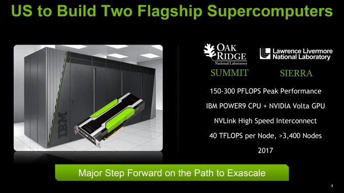
The launch of Oak Ridge National Laboratory’s Titan Supercomputer was in many ways a turning point for NVIDIA’s GPU compute business. Though already into their third generation of Tesla products by that time, getting Tesla into the world’s most powerful supercomputer is as much of a singular mark of “making it” as there can be. Supercomputer contracts are not just large orders in and of themselves, but they indicate that the HPC industry has accepted GPUs as reliable and performant, and is ready to significantly invest in them. Since then Tesla has ended up in several other supercomputer contracts, with Tesla K20 systems powering 2 of the world’s top 10 supercomputers, and Tesla sales overall for this generation have greatly surpassed the Fermi generation.
Of course while landing their first supercomputer contract was a major accomplishment for NVIDIA, it’s not the only factor in making the current success of Tesla a sustainable success. To steal a restaurant analogy, NVIDIA was able to get customers in the door, but could they get them to come back? As announced by the US Department of Energy at the end of last week the answer to that is yes. The DoE is building 2 more supercomputers, and it will be NVIDIA and IBM powering them.
The two supercomputers will be Summit and Sierra. At a combined price tag of $325 million, the supercomputers will be built by IBM for Oak Ridge National Laboratory and Lawrence Livermore National Laboratory respectively. They will be the successors to the laboratories respective current supercomputers, Titan and Sequoia.
Hardware
Both systems will be of similar design, with Summit being the more powerful of the two. Powering the systems will be a triumvirate of technologies; IBM POWER9 CPUs, NVIDIA Volta-based Tesla GPUs, and Mellanox EDR Infiniband for the system interconnect.

Starting with the CPU, at this point this is the first real attention POWER9 has received. Relatively little information is available on the CPU, though IBM has previously mentioned that POWER9 is going to emphasize the use of accelerators (specialist hardware), which meshes well with what is being done for these supercomputers. Otherwise beyond this we don’t know much else other than that it will be building on top of IBM’s existing POWER8 technologies.
Meanwhile on the GPU side, this supercomputer announcement marks the reintroduction of Volta by NVIDIA since going quiet on it after the announcement of Pascal earlier this year. Volta was then and still remains a blank slate, so not unlike the POWER9 CPU we don’t know what new functionality is due with Volta, only that it is a distinct product that is separate from Pascal and that it will be building off of Pascal. Pascal of course introduces support for 3D stacked memory and NVLink, both of which will be critical for these supercomputers.
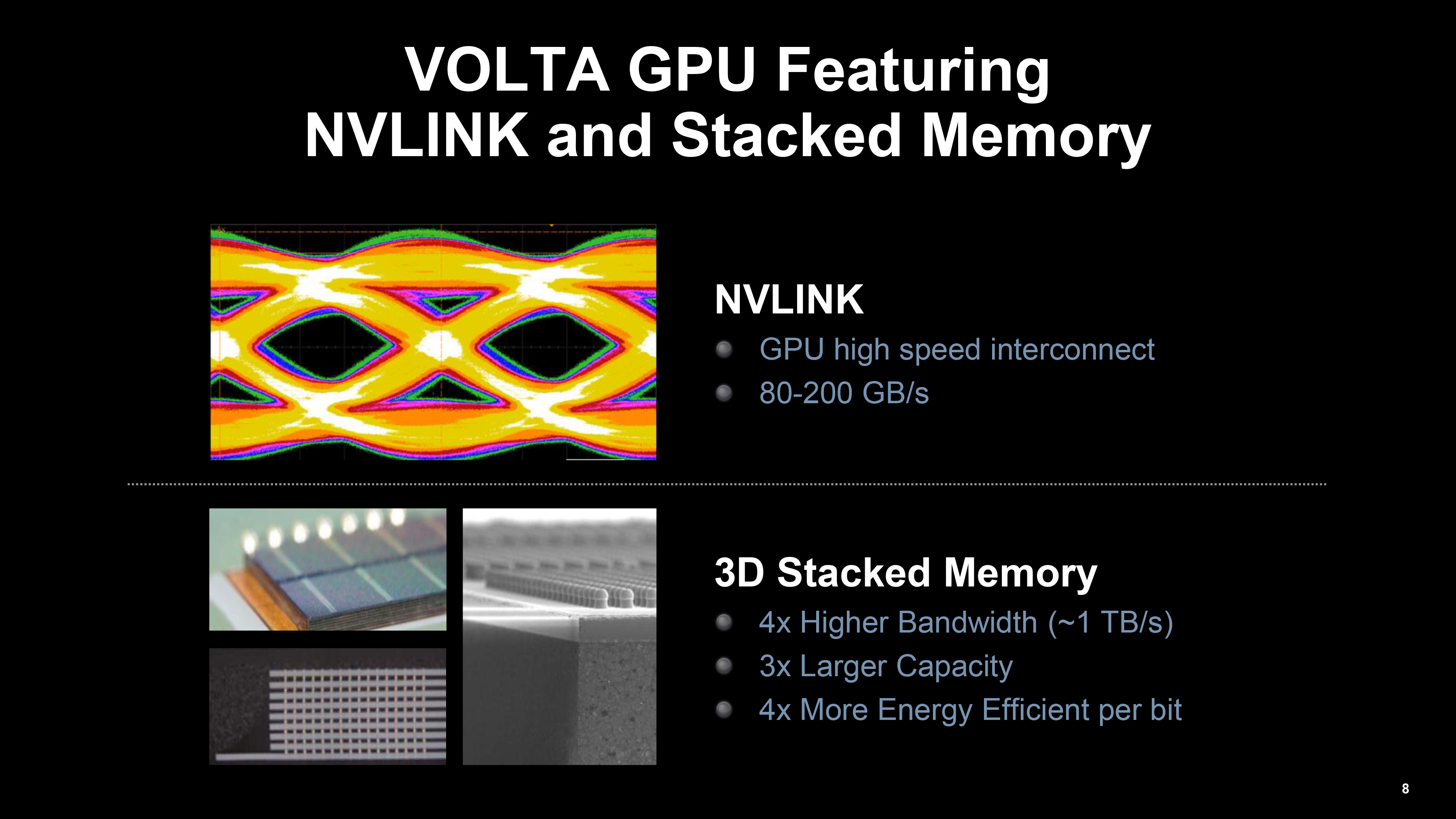
Speaking of NVLink, as IBM’s POWER family is the first CPU family to support NVLink it should come as no surprise that NVLink will be the CPU-GPU and GPU-GPU interconnect for these computers. NVIDIA’s high-speed PCIe replacement, NVLink is intended to allow faster, lower latency, and lower energy communication between processors, and is expected to play a big part in NVIDIA’s HPC performance goals. While GPU-GPU NVLink has been expected to reach production systems from day one, the DoE supercomputer announcement means that the CPU-GPU implementation is also becoming reality. Until now it was unknown whether an NVLink equipped POWER CPU would be manufactured (it was merely an option to licensees), so this confirms that we’ll be seeing NVLink CPUs as well as GPUs.
With NVLink in place for CPU-GPU communications these supercomputers will be able to offer unified memory support, which should go a long way towards opening up these systems to tasks that require frequent CPU/GPU interaction, as opposed to the more homogenous nature of systems such as Titan. Meanwhile it is likely – though unconfirmed – that these systems will be using NVLink 2.0, which as originally announced was expected for the GPU after Pascal. NVLink 2.0 introduces cache coherency, which would allow for further performance improvements and the ability to more readily execute programs in a heterogeneous manner.
Systems
| US Department of Energy Supercomputers | ||||||
| Summit | Titan | Sierra | Sequoia | |||
| CPU Architecture | IBM POWER9 | AMD Opteron (Bulldozer) |
IBM POWER9 | IBM BlueGene/Q | ||
| GPU Architecture | NVIDIA Volta | NVIDIA Kepler | NVIDIA Volta | N/A | ||
| Performance (RPEAK) | 150 - 300 PFLOPS | 27 PFLOPS | 100+ PFLOPS | 20 PFLOPS | ||
| Power Consumption | ~10MW | ~9MW | N/A | ~8MW | ||
| Nodes | 3,400 | 18,688 | N/A | N/A | ||
| Laboratory | Oak Ridge | Oak Ridge | Lawrence Livermore | Lawrence Livermore | ||
| Vendor | IBM | Cray | IBM | IBM | ||
Though similar in design, the total computational power and respective workloads will differ for Summit and Sierra. Sierra, the smaller of the systems, is to be delivered to Lawrence Livermore National Laboratory to replace their current 20 PetaFLOP Sequoia supercomputer. LLNL will be using Sierra for the National Nuclear Security Administration’s ongoing nuclear weapon simulations, with LLNL noting that “the machine will be dedicated to high-resolution weapons science and uncertainty quantification for weapons assessment.”
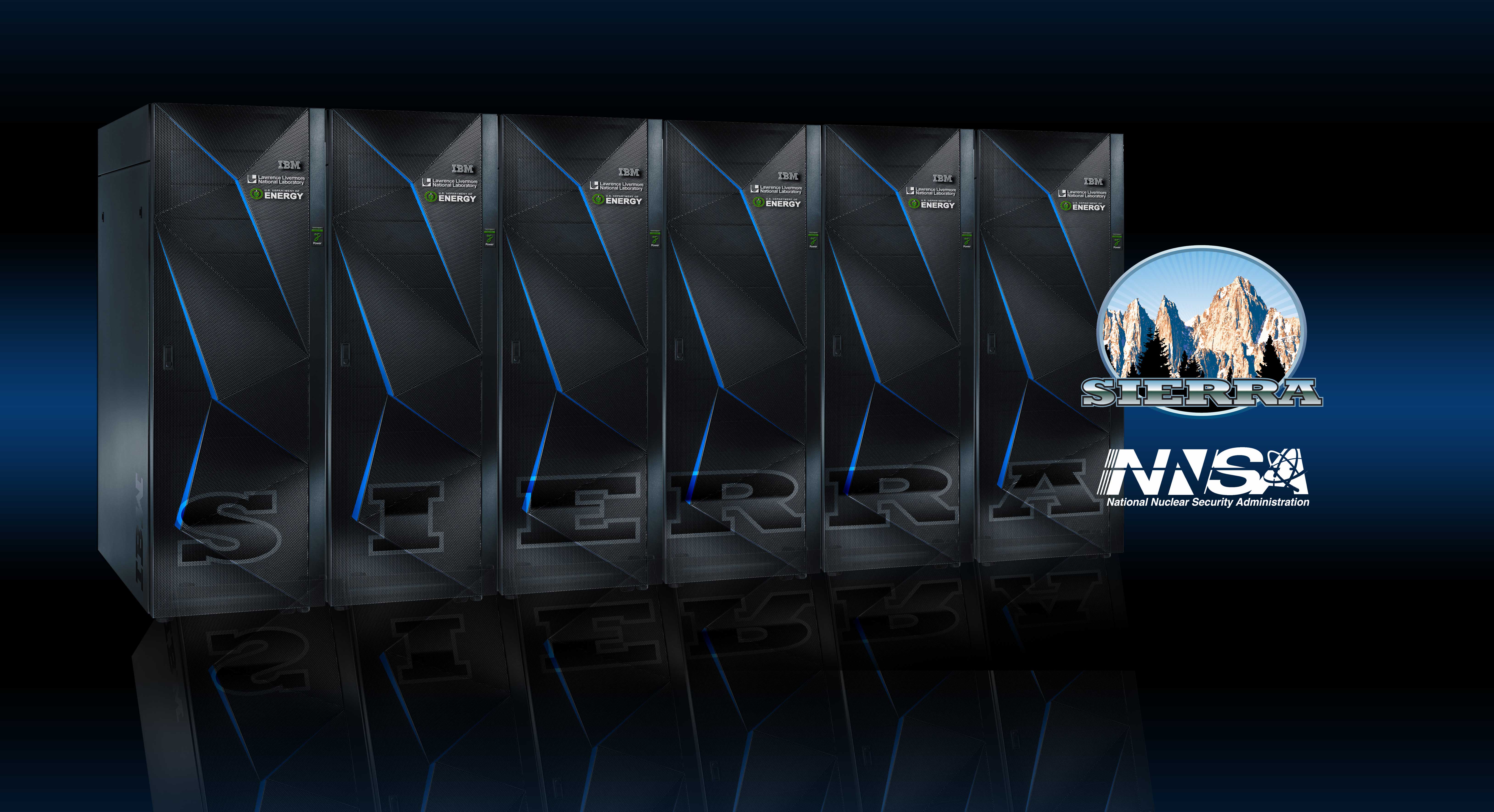
Sierra: 100+ PetaFLOPS
Due to its use in nuclear weapons simulations, information on Sierra is more restricted than it is for Summit. Publicly, Sierra is being quoted as offering 100+ PFLOPS of performance, over five-times the performance of Sequoia. As these supercomputers are still in development the final performance figures are unknown – power consumption and clockspeed cannot be guaranteed this early in the process, not to mention performance scaling on such a large system – and it is likely Sierra will exceed its 100 PFLOPS performance floor.
Meanwhile the more powerful of the systems, Summit, will be delivered to the Oak Ridge National Laboratory. In building their current Titan supercomputer, ORNL expected to get 4-5 years out of Titan, and adhering to that schedule Summit will be Titan’s replacement.
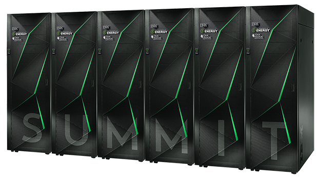
Summit: 150 to 300 PetaFLOPS
Summit’s performance is expected to be in the 150-300 PFLOPS range, once again varying depending on the final clockspeeds and attainable performance of the cluster. In 2012 ORNL wanted their next system to offer 10x the performance of Titan, and at this point Summit’s performance estimates range from 5x to 10x Titan, so while not guaranteed at this time it is still a possibility that Summit will hit that 10x goal.

As Summit is geared towards public work, we know quite a bit more about its construction than we do Seirra. Summit will be built out of roughly 3400 nodes, with each node containing multiple CPUs and GPUs (as opposed to 1 of each per Titan node). Each node in turn will be backed by at least 512GB of memory, most likely composed of 512GB of DDR4 and a to-be-determined amount of High Bandwidth Memory (stacked memory) on each GPU. Backing that in turn will be another 800GB of NVRAM per node.
From a power standpoint Summit is expected to draw 10MW peak, roughly 10% higher than Titan’s 9MW. However despite the slight increase in power consumption Summit is expected to physically be far smaller than Titan. With Summit nodes taking up roughly the same amount of space as Titan nodes, Summit’s nodes will occupy around only 20% of the volume of Titan’s nodes. Key to this of course is increasing the number of processors per node; along with multiple CPUs per node, NVIDIA’s new mezzanine form factor GPUs would play a large part here, as they allow for GPUs to be installed and cooled in a fashion similar to socketed CPUs, as opposeded to bulky PCIe cards.
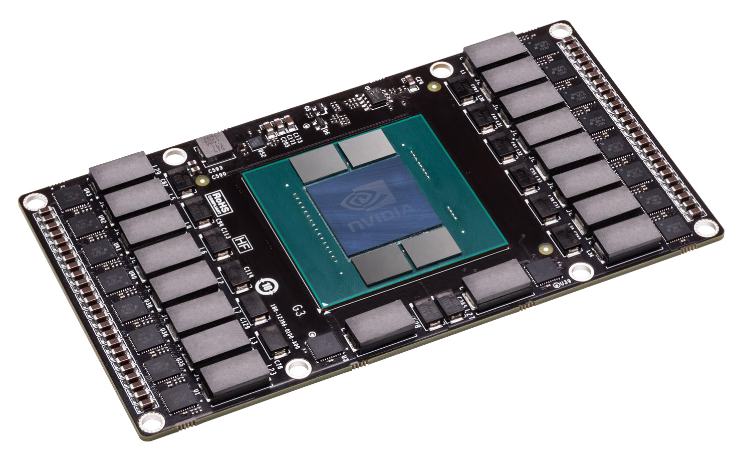
NVIDIA Pascal Test Vehicle Showing New GPU Form Factor
Like Titan before it, Summit will be dedicated to what ORNL calls “open science.” Time on the supercomputer will be granted to researchers through application proposals. Much of the science expected to be done on Summit is similar to the science already done on Titan – climate simulations, (astro)physics, nuclear, etc – with Summit’s greater performance allowing for more intricate simulations.
Finally, Summit is expected to come online in 2017, with trials and qualifications leading up to the machine being opened to users in 2018. As it stands, when Summit launches it will be the most powerful supercomputer in the world. Its 150 PLFOPS lower bound being roughly 3x faster than the current record holder, China’s Xeon Phi powered Tianhe-2, and no other supercomputers have been announced (yet) that are expected to surpass that number.
Wrapping things up, for both IBM and NVIDIA securing new supercomputer contracts is a major win. With IBM indirectly scaling back its role in the supercomputer race – BlueGene/Q being the last of the BlueGenes – IBM will continue providing supercomputers by providing heterogeneous powered by a mix of their own hardware and NVIDIA GPUs. NVIIDA of course is no less thrilled to be in not only the successor to Titan, but in another DoE lab’s supercomputer as well, and with a greater share of the underlying technology than before.
Though with that said, it should be noted that this is not the last major supercomputer order the DoE will be placing. The CORAL project for these supercomputers also includes a supercomputer for Argonne National Laboratory, who will be replacing their Mira supercomputer in the same timeframe. The details for that supercomputer will be announced at a later date, so there is still one more supercomputer contract to be awarded.


29 Comments
View All Comments
jwcalla - Monday, November 17, 2014 - link
I think the "unified memory" will be virtual, of course.przemo_li - Wednesday, November 19, 2014 - link
"unified" is technical term. Its mean "no translation" (without coherence), or "same point of view over data" (with coherence)."unified" as technical term thus do not mean "single thing"
"virtual" as technical term would mean that this "translation" is just hidden from developer.
Right now Nvidia have such "virtual" unified memory for their CUDA. Its not unified but driver takes care of translation.
Intel and some AMDs have unified memory without coherence. Memory can hold same values, and can be addressed by same methods, and can be seen by apps/os as single continuous address space. App developer just need to make sure that changed to data made in CPU are visible in GPU and vice versa.
AMD also have fully unified memory (hUMA), where data changed in CPU is instantly visible to GPU and vice versa without any app developer action.
Kevin G - Monday, November 17, 2014 - link
"Speaking of NVLink, as IBM’s POWER family is the first CPU family to support NVLink it should come as no surprise that NVLink will be the CPU-GPU and GPU-GPU interconnect for these computers."NVLink appears to be a variant of CAPI used in the POWER8 designs. They're both electrically PCIe with an encapsulated protocol on top.
What could change for the POWER9 is that IBM could move to optical links between processors which in turn would change CAPI. IBM, like Intel, has been researching silicon photonics for awhile now and this would be the first time they could produce a chip utilizing it. (IBM produced a massive optical hub for the HPC version of the POWER7 but it didn't use silicon photonics.)
The other amusing thing that this is the first big venture between IBM and nVidia since the Geforce 6800 (which IBM manufactured for nVidia). Times have certainly changed as both IBM and nVidia are now fabless companies.
BryanC - Monday, November 17, 2014 - link
NVLink is not electrically PCIe. It's a completely different signalling technology, more like what is described here:http://isscc.org/about/awards_2013.html
tipoo - Monday, November 17, 2014 - link
Is it known how many of those gflops come from the CPU side or the GPU side on those?SarahKerrigan - Monday, November 17, 2014 - link
According to the press release, "over 90%" of peak flops come from the GPU. The PPC component is very obviously there for serial sections - Amdahl's Law can be a harsh mistress.tipoo - Monday, November 17, 2014 - link
Makes sense, I expected it to be hugely GPU-leaning, even though the Power8s are some absolutely bonkers processors (in a good way).wurizen - Monday, November 17, 2014 - link
The reason why I want a PowerPC is that I buy it and 99% of you guys will not have it. And it's so powerful that I don't have to worry about roadmaps or updating it for a while. And, from the name "PowerPC," I should be able to run Crysis 3, and COD: Ghost at the same time. But, I know this will never happen. So, as long as a PowerPC is out there somewhere makes me hopeful somehow for some reason, which I don't know why.tipoo - Monday, November 17, 2014 - link
Outside of console-specific games which could not run on it either, Crysis and CoD would have x86 binaries that would not run on this (unless you did binary translation, but even then, the latency would likely be too much for a game, even if you have all this power at your disposal it's largely single threaded).So more likely, if you bought one, you'd be staring at a CLI display which looks like it's from the future the 70s conceived, and have absolutely no clue what to do with it by the sounds of things :P
tipoo - Monday, November 17, 2014 - link
Also you might already have "a powerpc", if you have an Xbox 360, Wii, Wii U, PS3, etc. They used PowerPC processors. Unless by "a powerPC", you meant the whole supercomputer shebang with thousands of powerPC processors in it, but doesn't make sense with the phrasing.