FMS 2014: Marvell Announces NVMe-Enabled PCIe 3.0 x4 88SS1093 SSD Controller
by Kristian Vättö on August 21, 2014 12:10 PM EST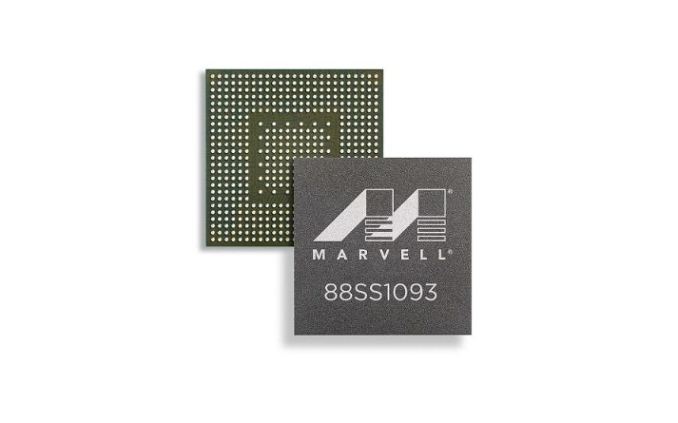
Two weeks ago Marvell announced their first PCIe SSD controller with NVMe support, named as 88SS1093. It supports PCIe 3.0 x4 interface with up to 4GB/s of bandwidth between the controller and the host, although Marvell has yet to announce any actual performance specs. While PCIe 3.0 x4 is in theory capable of delivering 4GB/s, in our experience the efficiency of PCIe has been about 80%, so in reality I would expect peak sequential performance of around 3GB/s. No word on the channel count of the controller, but if history provides any guidance the 88SS1093 should feature eight NAND channels similar to its SATA siblings. Silicon wise the controller is built on a 28nm CMOS process and features three CPU cores.
The 88SS1093 has support for 15nm MLC and TLC and 3D NAND, although I fully expect it to be compatible with Micron's and SK Hynix' 16nm NAND as well (i.e. 15nm TLC is just the smallest it can go). TLC support is enabled by the use of LDPC error-correction, which is part of Marvell's third generation NANDEdge technology. Capacities of up to 2TB are supported and the controller fits in both 2.5" and M.2 designs thanks to its small package size and thermal optimization (or should I say throttling).
The 88SS1093 is currently sampling to Marvell's key customers and product availability is in 2015. Given how well Intel's SSD DC P3700 fared in our tests, I am excited to see more NVMe designs popping up. Marvell has known to be the go-to controller source for many of the major SSD manufacturers (SanDisk and Micron/Crucial to name a couple), so the 88SS1093 will play an important part in bringing NVMe to the client market.


20 Comments
View All Comments
iwod - Thursday, August 21, 2014 - link
Finally, I have been waiting for two weeks for Anandtech to report this! Since other places aren't much good at discussing it."in our experience the efficiency of PCIe has been about 80%"
What causes that? I am pretty sure the PCIe has very low overhead.
I think this will be the next SSD for any current SSD owner to upgrade to. Since all current SSD are piratically limited by SATA. And May be its time for Apple to make their own firmware and SSD with this controller?
Kristian Vättö - Thursday, August 21, 2014 - link
"Finally, I have been waiting for two weeks for Anandtech to report this! Since other places aren't much good at discussing it."That's the reason why I'm not a big fan of live reporting at trade shows. As everyone is trying to be the first, I rather take my time and add some analysis instead of rewriting the PR. Too bad I didn't have the chance to meet with Marvell at FMS, so my details are limited to the PR :/
As for the PCIe efficiency, I'm not sure about that (yet). Based to my internal tests you can only get ~780MB/s out of a PCIe 2.0 x2 link and ~1560MB/s with x4, and Ryan, our GPU editor, confirmed similar efficiency with PCIe 3.0 with CUDA bandwidth.
From what I have heard, there are ways to increase the maximum bandwidth (which is why SF3700 is rated at up to 1.8GB/s with PCIe 2.0 x4) by playing with PCIe clock settings but I have yet to try that. I will definitely investigate this once we have more PCIe SSDs shipping.
repoman27 - Thursday, August 21, 2014 - link
It's due to protocol overhead and is directly related to the TLP Maximum Payload Size. Each Transaction Layer Packet has either a 12 or 16 byte header depending on whether it's 32 or 64-bit, optional ECRC which adds another 4 bytes, a 2 byte sequence number, LCRC which uses 4 bytes, and another couple bytes for framing. The TLPs are also interspersed with 8 byte Data Link Layer Packets at regular intervals. With a TLP Max Payload Size of 128 B, which is typical of current Intel desktop and mobile platforms, and provided no retransmissions, that works out to a theoretical peak efficiency of 2560 bytes of payload throughput for every 3112 bytes transferred, or ~82%. With larger maximum payload sizes, better efficiency can be achieved—up to 99% for a payload size of 4096 B.I really hope this controller provides for more than 8 channels, seeing as you would need 16 channels running at north of 200 MB/s apiece to hit the 3240 MB/s that a PCIe 3.0 x4 link is capable of.
Kristian Vättö - Thursday, August 21, 2014 - link
Thanks for the detailed explanation, it makes a lot more sense now.Most of the currently available NAND already support ONFI 3.0 or Toggle-Mode 2.0, which are good for up to 400MB/s per channel, so achieving 3GB/s should be possible even with an 8-channel design.
repoman27 - Thursday, August 21, 2014 - link
And a quick count shows the 88SS1093 package has 557 balls vs 400 for the 88SS9187, 320 for the 88SS1074, or 289 for the 88NV9145. So it could be a more than 8 channel design, or they actually expect the 400 MT/s NAND interfaces to deliver close to 400 MB/s.Stan11003 - Thursday, August 21, 2014 - link
From Wikipedia:PCIe 1.x uses an 8b/10b encoding scheme that results in a 20 percent ((10−8)/10) overhead on the raw bit rate. It uses a 2.5 GHz clock rate, therefore delivering an effective 250 000 000 bytes per second (250 MB/s) maximum data rate.
This scheme was used for PCIe 2.x also lucky for all of us PCIe 3.0 has a new scheme.
PCI Express 3.0 upgrades the encoding scheme to 128b/130b from the previous 8b/10b encoding, reducing the overhead to approximately 1.54% ((130–128)/130), as opposed to the 20% overhead of PCI Express 2.0. This is achieved by a technique called "scrambling" that applies a known binary polynomial to a data stream in a feedback topology. Because the scrambling polynomial is known, the data can be recovered by running it through a feedback topology using the inverse polynomial. PCI Express 3.0's 8 GT/s bit rate effectively delivers 985 MB/s per lane, practically doubling the lane bandwidth relative to PCI Express 2.0.[21]
repoman27 - Thursday, August 21, 2014 - link
The 80% number Kristian referred to is on top of the loss due to encoding efficiency. But yes, PCIe 2.0 is really 4 Gbit/s per lane because of 8b/10b encoding, yet PCIe 3.0 is still 7.877 Gbit/s (close to the nominal 8 Gbit/s) because of the switch to 128b/130b.DIYEyal - Thursday, August 21, 2014 - link
Finally, the NVMe revolution begins.. (I'm aware it's not the first product, but it's good to see more NVMe controllers), although this seems like it's targeted more towards M.2 SSDs rather than desktop PCIe cards..frenchy_2001 - Friday, August 22, 2014 - link
There is absolutely no difference from a controller perspective between the form factors: both use PCIe interface and will deliver data over the NVMe protocol. M.2 is limited to 4x lanes at up to Gen3 while a PCIe card could use up to 16x lanes Gen3. As this controller is limited to x4 anyway, no restriction... (as a comparison, Intel SF3700 uses a Gen3 x4 controller too and is sold in PCIe card format only so far).MrSpadge - Thursday, August 21, 2014 - link
This could be a nice competitor to SF3700. And I'd love to see a MX100-style drive based on this :)