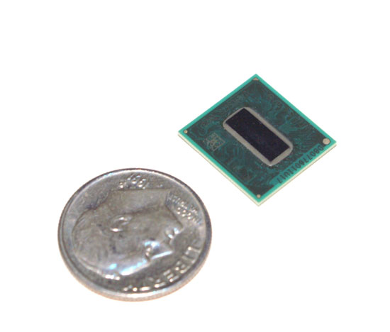
Intel's Atom Architecture: The Journey Begins
by Anand Lal Shimpi on April 2, 2008 12:05 AM EST- Posted in
- CPUs
The Atom processor's architecture is not about being the fastest, but being good enough for the tasks at hand. A product like ASUS' EeePC would not have existed 5 years ago, the base level of system performance simply wasn't great enough. These days, there's still a need for faster systems but there's also room for systems that aren't pushing the envelope but are fast enough for what they need to do.
The complexity of tasks like composing emails, web browsing and viewing documents is increasing, but not at the rate that CPU performance is. The fact that our hardware is so greatly outpacing the demands of some of our software leaves room for a new class of "good enough" hardware. So far we've seen a few companies, such as ASUS, take advantage of this trend but inevitably Intel would join the race.
One of my favorite movies as a kid was Back to the Future. I loved the first two movies, and naturally as a kid into video games, cars and technology my favorite was the second movie. In Back to the Future II our hero, Marty McFly, journeys to the future to stop his future son from getting thrown in jail and ruining the family. While in the future he foolishly purchases a sports almanac and attempts to take it back in time with him. The idea being that armed with knowledge from the future, he could make better (in this case, more profitable) decisions in the past.
I'll stop the analogy there because it ends up turning out horribly for Marty, but the last sentence sums up Intel's approach with the Atom processor. Imagine if Intel could go back and remake the original Pentium processor, with everything its engineers have learned in the past 15 years and build it on a very small, very cool 45nm manufacturing process. We've spent the past two decades worrying about building the fastest microprocessors, it turns out that now we're able to build some very impressive fast enough microprocessors.
The chart below tells an important story:
| Manufacturing Process | Transistor Count | Die Size | |
| Intel Pentium (P5) | 0.80µm | 3.1M | 294 mm^2 |
| Intel Pentium Pro (P6) | 0.50µm | 5.5M* | 306 mm^2* |
| Intel Pentium 4 | 0.18µm | 42M | 217 mm^2 |
| Intel Core 2 Duo | 65nm (0.065µm) | 291M | 143 mm^2 |
| Intel Core 2 Duo (Penryn) | 45 nm | 410M | 107 mm^2 |
In 1993, it took a great deal of work for Intel to cram 3.1 million transistors onto a near 300 mm^2 die to make the original Pentium processor. These days, Intel manufacturers millions of Core 2 Duo processors each made up of 410 million transistors (over 130 times the transistor count of the original Pentium) in an area around 1/3 the size.
Intel isn't stopping with Core 2, Nehalem will offer even greater performance and push transistor counts even further. By the end of the decade we'll be looking at over a billion transistors in desktop microprocessors. What's interesting however isn't just what Intel can do to push the envelope on the high end, but rather what Intel can now do with simpler designs on the low end.

What's possible today on 45nm...
With a 294 mm^2 die size, Intel could not manufacture the original Pentium for use in low cost devices however, today things are a bit different. Intel doesn't manufacture chips on a gigantic 0.80µm process, we're at the beginnings of a transition to 45nm. If left unchanged, Intel could make the original Pentium on its latest 45nm process with a die size of less than 3 mm^2. Things get even more interesting if you consider that Intel has learned quite a bit in the past 15 years since the debut of the original Pentium. Imagine what it could do with a relatively simple x86 architecture now.


46 Comments
View All Comments
lopri - Thursday, April 3, 2008 - link
This article is as much propagana-ish as it is technical. Did you read the last page of the article?clnee55 - Friday, April 4, 2008 - link
Since Anand wrote this article. I let him answer your accusationGulWestfale - Wednesday, April 2, 2008 - link
i believe that the graphics core in the chipset is a powerVR gen5 derivative; intel already uses some of their tech in its existing mainboards and wikipedia states that intel has licensed gen5 tech for one of its chipsets, the GMA500 (which is the same as poulsbo?) gen5 is also DX10-capable, which matches the info in your article.http://en.wikipedia.org/wiki/PowerVR#Series_5_.28S...">http://en.wikipedia.org/wiki/PowerVR#Series_5_.28S...
yyrkoon - Wednesday, April 2, 2008 - link
and wikipedia has been known to be wrong . . . a lot lately it seems.My point here *is*, I would probably trust anandtech more than wikipedia now days, as it seems any Joe can put up a 'reference' without citation.
jones377 - Wednesday, April 2, 2008 - link
Following the references link from the Wiki article...http://www.imgtec.com/News/Release/index.asp?NewsI...">http://www.imgtec.com/News/Release/index.asp?NewsI...
Poulsbo uses a PowerVR 3D core
Anand Lal Shimpi - Wednesday, April 2, 2008 - link
Yep, you guys are correct, I wasn't aware that it was public yet :) I've updated the article.Take care,
Anand