PCI Express 2.0: Scalable Interconnect Technology, TNG
by Kris Boughton on January 5, 2008 2:00 AM EST- Posted in
- CPUs
Intel Chipset PCI Express Resource Assignments
Intel desktop platforms make use of a pair of bus controllers, commonly referred to as the chipset. The Memory Controller Hub (MCH) or "Northbridge" (NB) is responsible for directly interfacing the processor with memory as well as all other system resources, and it communicates all information to the CPU over the Front Side Bus (FSB). The memory controller, which makes up a portion of the MCH, is responsible for arbitrating requests for bus time and translating requests for data located in system memory into the appropriate commands and addresses needed to retrieve and deliver that information to the CPU and other DMA (Direct Memory Access) devices. This discussion, although relevant to understanding the operation of the MCH, is better left for another day. Instead, we would like to concentrate on the second major function of the Northbridge, which is providing PCI Express ports for lane assignments and data transfers. Incorporating the PCI Express controller into the Northbridge ensures that installed graphics cards have easy access to system memory and CPU resources.
The Northbridge communicates with the I/O Controller Hub (ICH), or "Southbridge", using an interface that Intel calls Direct Media Interface (DMI) at a maximum transfer rate of 2GB/s. This connection is actually nothing more than a PCI Express x4 link with a dedicated transaction layer which handles routing of all input/output (I/O) data from attached peripherals such as hard disks, optical drives, Ethernet controllers, onboard audio, and Universal Serial Bus (USB) and PCI devices. The Intel 875/ICH5 chipset, the last to make use of then-aging AGP technology, made use of a PCI link in this location which provided only 266MB/s (133MB/s in each direction) total bandwidth. The 915/ICH6 "Express" chipset was the first to make use of this higher speed link - a change that improved the performance of technologies such as SATA (both 1.5Gbps and 3.0Gbps) and onboard 1Gbps Ethernet ports, giving them the headroom they need to function at their maximum potential.
Each PCI Express "Port" in the Northbridge is actually a pre-configured x4 lane (meaning that lane resources can only be assigned in chunks of four). The table below shows the PCI Express resources available from some of the more recent Intel chipsets. Reviewing this we see that the only real difference between the older 965P and 975X chipset, in term of graphics capabilities, was the ability for the 975X chipset to split the available x16 lane into two x8 lanes for CrossFire configurations. This difference was more than likely for market distinction and not a true limitation of the chipset. PCI Express is highly scalable and there is no obvious reason as to why 2x8 CrossFire on a P965 chipset should not work. Much like P965, P35 is limited to single x16 configurations.
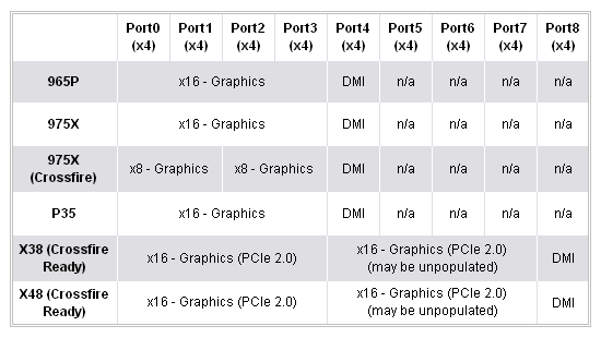
The real change comes with the introduction of Intel's current X38 flagship chipset. The X38 chipset provides two true PCI Express 2.0 capable x16 lanes for use with the latest PCI-E 2.0 graphics cards. A pair of ATI/AMD graphics cards in CrossFire will receive a full 16 lanes of bandwidth each regardless of the PCI Express specification they use - the only difference is the maximum theoretical throughput (16GB/s with PCI-E 2.0 and 8GB/s with PCI-E 1.x). Future X48 chipsets, which appear to be speed-binned X38 chipsets, will provide exactly the same capabilities.
Some 975X users may have asked themselves if it was possible to "unlock" x16 link speeds for their two graphics cards running in CrossFire - if one card can run at x16 speed, why not two? (The slots are certainly big enough to house the cards and all the right traces are on the motherboard.) As we can see, the chipset is physically incapable of that configuration as the PCI Express resources needed to form two x16 links simply are not there - there is nothing to change and nothing to re-configure.
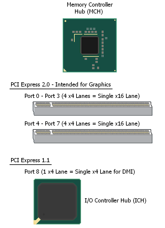
In the case of each "Express" chipset, a final x4 port is available for the purposes of linking the Southbridge to the Northbridge. Although the X38/X48 chipsets are true PCI Express 2.0 parts, they configure Port8 for PCI Express 1.x speeds, as the ICH9(R) Southbridge is only a PCI Express 1.x enabled part. As such, we expect that Intel's upcoming ICH10(R) will make full use of PCI-E 2.0 as well meaning that the associated DMI connection should see a nice boost in speed to 4GB/s (double that of today). Below is a simple physical representation of the X38/X48 PCI Express resources.
PCI Express 2.0 to 1.x backwards-compatibility allowed Intel the opportunity to release a PCI Express 2.0 MCH now with an ICH to follow, something that would not have been possible otherwise. Traditionally we see a new ICH at the same time as the MCH. Given the extra time Intel has for the refinement of ICH10(R), we will be satisfied with nothing less than perfection.
The ICH provides the system with an additional six PCI Express 1.x lanes (to be grouped as desired by the motherboard design company). However, as we have seen, the DMI link is capable of sustaining a maximum throughput of x4 speed to the Northbridge. This means that in the case of fully populated link states a lot of the bandwidth originating from downstream-attached peripherals is bottlenecked if outputting anything more than short bursts of data. Coincidentally, this is why pseudo-CrossFire configurations on P965 and P35 chipsets are limited to x4 speeds for the second card (additionally, x6 link states are not allowed). For the same reasons, the use of a third graphics card in X38/X48 configurations for physics acceleration purposes sees the same limitation. Previous testing indicates that there may be a slight performance penalty associated with x16/x4 CrossFire compared to x8/x8 or x16/x16 solutions, but despite having less than one fourth the bandwidth we do not see a massive loss of performance. In other words, we are definitely not at the point yet where we are using all of the available bandwidth for even PCI-E 1.x x16 slots.


21 Comments
View All Comments
rogerdpack - Monday, July 23, 2012 - link
So shouldn't the article list PCIe 2.0 throughput as 400 MB/s because of the 8b/10b encoding overhead?