Kioxia and Western Digital Debut 218-Layer 3D NAND: 1Tb TLC with 3.2 GT/s IO Speed
by Anton Shilov on March 31, 2023 12:00 PM EST
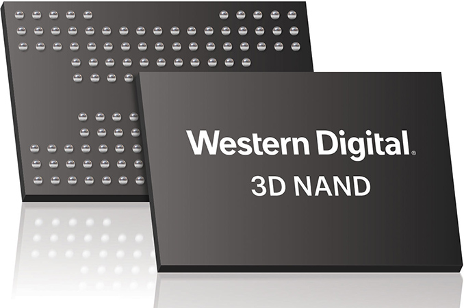
Kioxia and Western Digital formally introduced their 8th Generation BiCS 3D NAND memory with 218 active layers. The new storage device offers a 1Tb capacity in 3D TLC mode and features 3200 MT/s data transfer speed, a combination that will enable SSD makers to build high-performance, high-capacity drives. To enable such an extreme interface speed, the companies adopted an architecture akin to YMTC's Xtacking.
The 218-layer BiCS 3D NAND device jointly developed by Kioxia and Western Digital supports triple-level cell (TLC) and quad-level cell (QLC) configurations to maximize storage density and expand addressable applications. The companies said that the new device embraces their new 'lateral shrink technology to increase bit density by over 50' without elaborating. Considering that the flash memory IC increased the number of active layers by 34%, the claim about a 50% bit density increase indicates that developers also shrank lateral sizes of NAND cells to fit in more of them per layer.
Meanwhile, the 218-layer 3D NAND device features a quad-plane architecture allowing for a higher level of parallelism for programming and read times and increased performance. In addition, the 218-layer 3D TLC device also has a 3200 MT/s (which could provide a 400 MB/s peak read/write speed) input/output interface, which is the highest I/O speed announced so far. High data transfer rates will be handy for high-end client and enterprise SSDs featuring a PCIe 5.0 interface.
The key innovation of the 8th Generation BiCS 3D NAND memory is the all-new CBA (CMOS directly Bonded to Array) architecture that implicates separate production of 3D NAND cell array wafers and I/O CMOS wafers using the most optimal process technologies and then bonding them together to create a final product that offers increased bit density and fast NAND I/O speed. Meanwhile, Kioxia and Western Digital must disclose details about their CBA architecture and whether the I/O CMOS wafers carry other NAND peripheral circuitry, like page buffers, sense amplifiers, and charge pumps.
Producing memory cells and peripheral circuits separately solves several problems as it allows manufacturers to make them using the most efficient process technologies in their sections of cleanrooms. This brings further benefits as the industry adopts methods like string stacking.

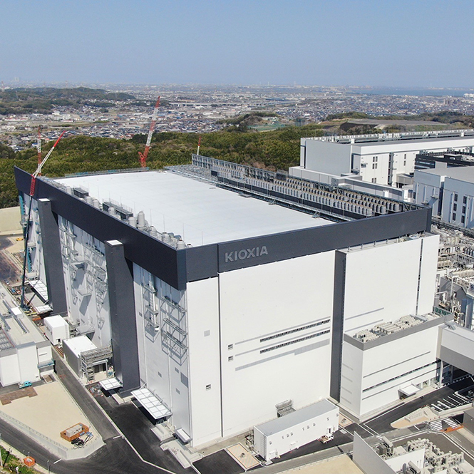
Kioxia and Western Digital Fab 7, Yokkaichi Plant, Japan
Kioxia said it had started sample shipments of 8th Generation BiCS 3D NAND memory devices to select customers. Still, there is no word when the company expects to initiate volume production of its next-generation flash memory. It is not unusual for companies to announce new types of 3D NAND quarters before they enter mass production, so it is reasonable to expect 8th Gen BICS on the market in 2024.
"Through our unique engineering partnership, we have successfully launched the eighth-generation BiCS Flash with the industry's highest bit density," said Masaki Momodomi, Chief Technology Officer at Kioxia Corporation. "I am pleased that Kioxia's sample shipments for limited customers have started. By applying CBA technology and scaling innovations, we've advanced our portfolio of 3D flash memory technologies for use in various data-centric applications, including smartphones, IoT devices, and data centers."


34 Comments
View All Comments
sheh - Friday, March 31, 2023 - link
Layer count comparison:https://blocksandfiles.com/2023/03/31/kioxia-and-w...
PeachNCream - Friday, March 31, 2023 - link
Great a die shrunk TLC NAND chip. I'm sure the lack of detail about P/E endurance is not at all an indicator of further reductions in useful lifespan at all. Nope, not even a little bit. Instead please pay attention to performance specs.ballsystemlord - Friday, March 31, 2023 - link
And how about retention after power-down? I've yet to hear anything about that for QLC flash nor for many of the newer TLC flash chips.sheh - Saturday, April 1, 2023 - link
@ballsystemlordPresumably, meeting the JEDEC specs. Other than that I don't recall ever seeing anyone publish detailed info on retention.
back2future - Saturday, April 1, 2023 - link
e.g.2015 technology level https://www.anandtech.com/show/9248/the-truth-abou...
2018 QLC (market entry) expectations, article endurance (TBW) and comments data retention? (year(s)) https://www.anandtech.com/show/13078/the-intel-ssd...
2021 FerriSSDs (?) https://www.eetimes.com/silicon-motions-ferrissd-h... ("At higher temperatures, NAND Flash memory cells age faster, so the duration of data retention falls faster.", but have a look at Jedec specification with increasing data retention on higher active temp(eratures) for client/enterprise (?) )
sheh - Sunday, April 2, 2023 - link
These are just models and extrapolations. Now that we've had consumer SSDs for 15 years it's time someone published concrete real life data.The Tech Report RIP did an SSD endurance test back then, but conducting retention tests is much difficult.
(If you go looking for the retention articles, brace yourself. The site was purchased a few years ago and turned into a random crypto-gambling-clickbait cesspool.)
back2future - Monday, April 3, 2023 - link
A 2020 summary for results between 3d-TLC and QLC flash ("The errors and the optimal read voltages of 3D TLC and QLC flash-memory chips are explored.") might be a starting point ( https://www.microarch.org/micro53/papers/738300a48... ) although it seems pretty theoretical results considering looking for consumer friendly review or summary on data retention parameters and storage treatment recommendations.I do agree, public data on data retention seems rare considering market share of SSDs nowadays.
ballsystemlord - Tuesday, April 4, 2023 - link
back2future & shehThanks for trying to look into this matter. I did try and research it a few years ago with about the same success you two have had.
The 2015 AT article was from one manufacturer (Intel) many many years ago and I think it was for planar flash, and before stacking, and before QLC came out, and before we changed the cell type to charge trap flash.... so not really that useful.
The 2018 QLC comment section and 2021 FerriSSDs articles are just some off hand comments and an advertisement of a product intended for the auto market. The JEDEC standard I think is JESD219A. It costs as much as a 1TB PCIe 4.0 flash drive to obtain, just so I know about how long my SSDs will retain their data -- and I probably have to sign an agreement not to tell anyone else about data-retention. When will the tech world learn to give us some hard data?! What happened to science being important?! Is it only for their exclusive club?!
The Infineon paper you cite is talking about floating gate flash which, AFAIK, is not used in modern consumer flash products. They don't test anything in their other than storing the drive at 85C, which how long it retains data is based on how many times it was P/E (Programmed and Ereased).
Regarding your IEEE article, that's the most interesting of the bunch. I'll have to read that later...
ballsystemlord - Tuesday, April 4, 2023 - link
EDIT: Regarding the Infineon paper, (AFAIK) it's 85C they're testing at, 55C real world operating conditions. I.E. cold storage isn't taken into consideration -- and as you might recall from the Intel post you cited from AT, 55C is the absolute best case scenario. Even Intel, back then, got ~8 years of data retention in that bast case scenario.See section 3.1, third paragraph from the bottom.
back2future - Wednesday, April 5, 2023 - link
2015 article is real information with look-up tables from JEDEC standard for hardware that time (if there's smth. like that for 202x QLC Nand flash comparing development of retention and hardware qualities was possible?), 2018 shows steady interest on retention, but only on commenters sections (being one example on that maybe biased view) and FerriSSDs being one example for technology dev.s to remedy short data retention specs (another was reheating flash cells having high P/E cycle numbers for curing defects and somewhat extremely extending P/E cycles, IIRC from 1-10k (~MLC or TLC flash classes) to <1-100M, but only theoretical considerations made on that approach)55°C is highest temperature for active device on JEDEC (Intel) table, enabling highest ~400 weeks data retention (on SLC/MLC types?) with steady(?)/average 25°C storage temperatures.
Me, no flash gate differences, nor production node sizes considered with researching some overview information.
Infineon and IEEC abstract correlate on information towards each other (~1k years endurance for 1time or low W/E cycles, but seems nonsense expecting linearity for a 1k years retention within diagram figure6, i'ld absolutely agree on that point) for Infineon with probably 2d SLC or MLC flash cells (10k-100k P/E endurance mentioned).
What's data retention for HDD's, current USB flash devices, sd-cards or M.2&NVME Nand storage devices (, DVD or Bluray)?