Startup Showcases 7 bits-per-cell Flash Storage with 10 Year Retention
by Dr. Ian Cutress on December 15, 2021 11:30 AM EST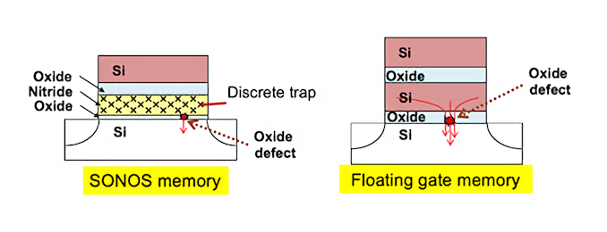
One of the key drivers to increase capacity in next generation storage has been to increase the number of bits that can be stored per cell. The easy jump of one to two bits-per-cell gives a straight 100% increase, in exchange for more control needed to read/write the bit but also limits the cell endurance. We’ve seen commercialization of storage up to four bits-per-cell, and talk about five. A Japanese company is now ready to start talking about their new 7 bits-per-cell solution.
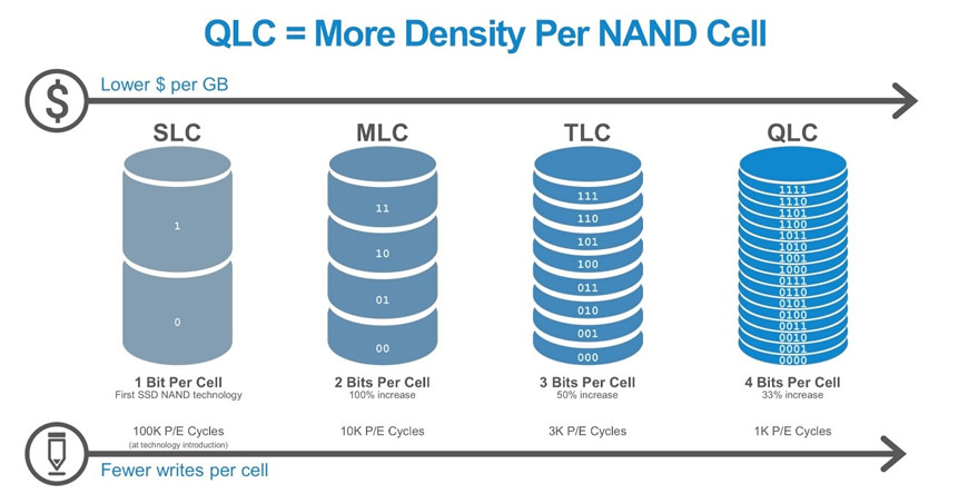
Image courtesy of Plextor, up to 4 bits-per-cell
Moving from one to two bits-per-cell gives an easy doubling of capacity, and moving to three bits-per-cell is only another 50% increase. As more bits are added, the value of adding those bits diminishes, but the cost in the equipment to control the read and writes increases exponentially. There has to be a medium balance between how many bits-per-cell makes economic sense, and how much the control electronics costs to implement to enable those bits.
- 1 bit per cell requires detection of 2 voltage levels, base capacity
- 2 bit per cell requires detection of 4 voltage levels, +100% capacity
- 3 bit per cell requires detection of 8 voltage levels, + 50% capacity
- 4 bit per cell requires detection of 16 voltage levels, +33% capacity
- 5 bit per cell requires detection of 32 voltage levels, +25% capacity
- 6 bit per cell requires detection of 64 voltage levels, +20% capacity
- 7 bit per cell requires detection of 128 voltage levels, +16.7% capacity
Also, the more bits-per-cell, the lower the endurance – the voltage variation when you store many bits only has to drift slightly to get the wrong result, and so repeated read/writes to a high capacity cell will make that voltage drift until the cell is unusable. Right now the market seems happy with three bits-per-cell (3bpc) for performance and four bits-per-cell (4bpc) for capacity, with a few 2bpc designs for longer term endurance. Some of the major vendors have been working on 5bpc storage, although the low endurance may make the technology only good for WORM – write once, read many, which is a common acronym for the equivalent of something like an old-school CD or non-rewritable DVD.

Floadia Corp., a Series C startup from Japan, issued a press release this week to state that it has developed storage technology capable of seven bits-per-cell (7bpc). Still in the prototype stage, this 7bpc flash chip, likely in a WORM scenario, has an effective 10-year retention time for the data at 150C. The company says that a standard modern memory cell with this level of control would only be able to retail the data for around 100 seconds, and so the secret in the design is to do with a new type of flash cell they have developed.
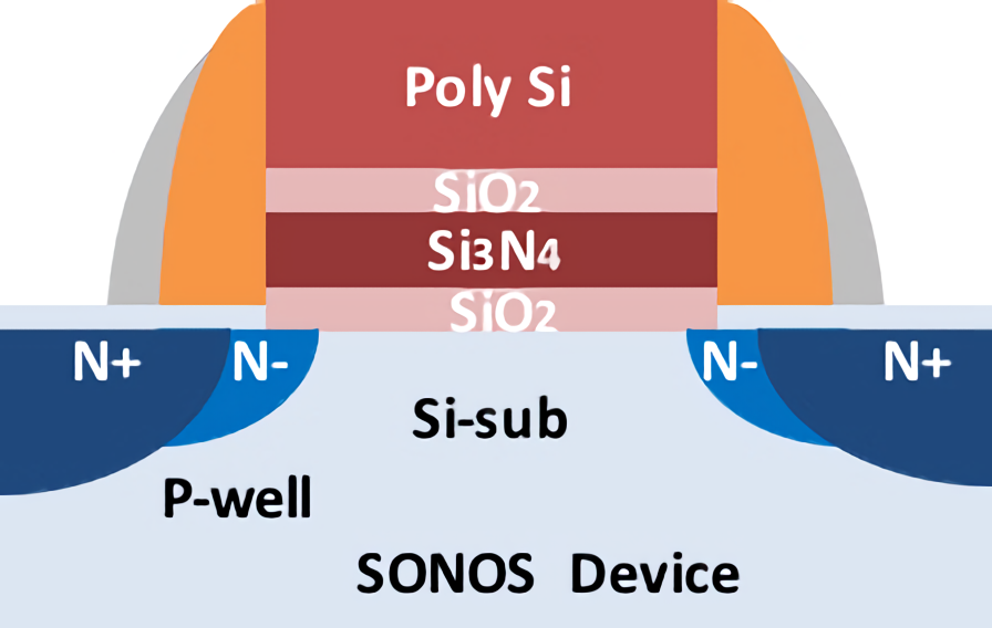
The SONOS cell uses a distributed charge trap design relying on a Silicon-Oxide-Nitride-Oxide-Silicon layout, and the company points to an effective silicon nitride film in the middle where the charges are trapped to allow for high retention. In simple voltage program and erase cycles, the company showcases 100k+ cycles with a very low voltage drift. The oxide-nitride-oxide layers rely on SiO2 and Si3N4, the latter of which is claimed to be easy to manufacture. This allows a non-volatile SONOS cell to be used in NV-SRAM or embedded designs, such as microcontrollers.
It’s actually that last point which means we’re a long time from seeing this in modern NAND flash. Floadia is currently partnering with companies like Toshiba to implement the SONOS cell in a variety of microcontrollers, rather than large NAND flash deployments, at the 40nm process node as embedded flash IP with compute-in-memory properties. Those aren’t at 7 bits-per-cell yet, to the effect that the company is promoting that two cells can store up to 8-bits of network weights for machine learning inference – when we get to 8 bits-per-cell, then it might be more applicable. The 10-year retention of the cell data is where it gets interesting, as embedded platforms will use algorithms with fixed weights over the lifetime of the product, except for the rare update perhaps. Even with increased longevity, Floadia doesn’t go into detail regarding cyclability at 7bpc at this time.
An increase from modern 3bpc to 6bpc NAND flash would afford a double density increase, however larger cells would be needed, which would negate the benefits. There’s also the performance aspect if the development of >4bpc ever made it to consumers, which hasn’t been touched upon.
It will be an interesting technology to follow.
Source: Floadia Press Release


48 Comments
View All Comments
back2future - Sunday, December 19, 2021 - link
please delete https://www.anandtech.com/comments/17116/startup-s...mode_13h - Monday, December 20, 2021 - link
LOL, yeah. That didn't work too well.Surprisingly, I managed to copy and paste it to a file, then base64 -d and get an *almost* valid JPG file. I'm just missing the X-axis label in your graph.
back2future - Tuesday, December 21, 2021 - link
possible also, inserting from data:image/jpeg;base64,/9j/4AAQSkZ...31KRFKUpE/9k= into browser address line (url for uniform resource identifier)( links without colons or bracket are functional also )
back2future - Sunday, January 2, 2022 - link
and knowing everything about YOU now :)('profiling' done, and interesting to know: https://app.rebrandly.com/public/links/share?href=... )
PaulHoule - Friday, December 31, 2021 - link
I am wondering if they are ever going to go to some number of levels which isn't a power of two. For instance you might be better off going from 16 levels to 25 levels instead of 32 levels, particularly if you are tuning dynamically for performance, persistence, device aging, etc.At the block level I don't see any problem being non-binary because you can arithmetic code your data. I know it is hard to parallelize but it doesn't seem too hard if you could lean on the main CPU instead of depending on inferior silicon in the device or put some small, specialized and fast-clocked chiplet into the device.
mode_13h - Friday, December 31, 2021 - link
> wondering if they are ever going to go to some number of levels which isn't a power of two.It might come to that, if 5-bit cells prove too challenging.
> At the block level I don't see any problem being non-binary
Yeah, I think that's not the main issue. As the article pointed out, the benefit of each additional bit per cell decreases exponentially, yet the tradeoffs are real. Once you start adding *fractions* of a bit per cell, the upside is even smaller. Maybe for like bottom-tier NAND, used in the lowest-margin products, it might still be worthwhile.
Another doubt I have is about the ADC technology you'd need to use. Naively, I think you'd need at least a 6-bit ADC to recover 4.5 bits of information per cell. However, maybe there's some way to build a non- base-2 ADC that would be more cost-effective.
Tomatotech - Saturday, January 1, 2022 - link
I’m guessing that the vast majority of data on SSD is actually static data that rarely changes from month to month (or even year to year).I wouldn’t mind an 8 TB m.2 drive where 4 or 6 TB is ultra cheap low cycle 7-bit storage, and 2-4 TB is faster / more durable SLC or MLC. Of course that requires more intelligent tiered storage monitoring brains on the m.2 drive but it seems feasible.
I don’t fully understand how it works but many modern nvme SSDs shift their storage between SLC / TLC / QLC as needed so if it’s possible to extend that further, I’d be happy with a nvme drive that shifted its storage space between 7+-bit long term storage and SLC as needed. Yes this means the capacity varies dynamically - this already happens behind the scenes with modern SSDs. Also over time some cells might become too degraded to be available for 7+-bit storage. They can just be redesigated as permanent SLC (or xLC) cells.
back2future - Sunday, January 2, 2022 - link
with customers getting information about wear leveling, TBW (with smart output) and long term storage capabilities of currently available flash cells within storage devices?Easy example: How does one get wear information on sdxc or sduc (<=128TB, ~GB/s) secure digital cards?