MediaTek Announces Dimensity 9000: Supercharged Flagship SoC on 4nm
by Andrei Frumusanu on November 18, 2021 6:00 PM EST5th Generation APU/NPU, a Massive ISP, and New 5G & WiFi
APU/NPU AI/ML Upgrades
Moving away from CPU and GPU, we find MediaTek’s new “APU”, or AI Processing Unit, or rather NPU as we more generically tend to call it nowadays. MediaTek always had one of the earliest in-house implementations of such an IP, and the Dimensity 9000 now implements the 5th generation of such an IP.
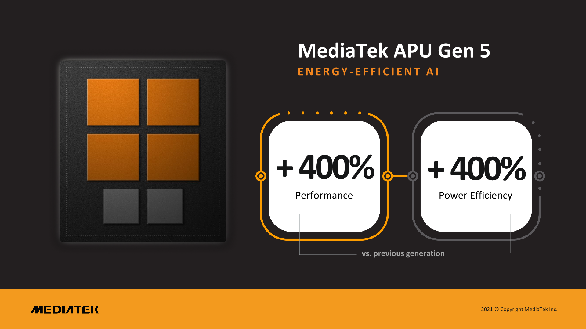
MediaTek promises a +400% performance and power efficiency improvement over the previous generation Dimensity 1200 implementation, which is quite a step-up, however should be contextualised to other more performant competitor platforms.
The company had made one slide available of showcasing MLPerf against Apple’s A15, noting +108% at +75% power efficiency versus the iPhone chip, the company here actually quoted our own published MLPerf figures, however we’ll avoid using the slide as the comparison isn’t great as the iOS variant of the app isn’t fully optimised and doesn’t take advantage of CoreML acceleration.
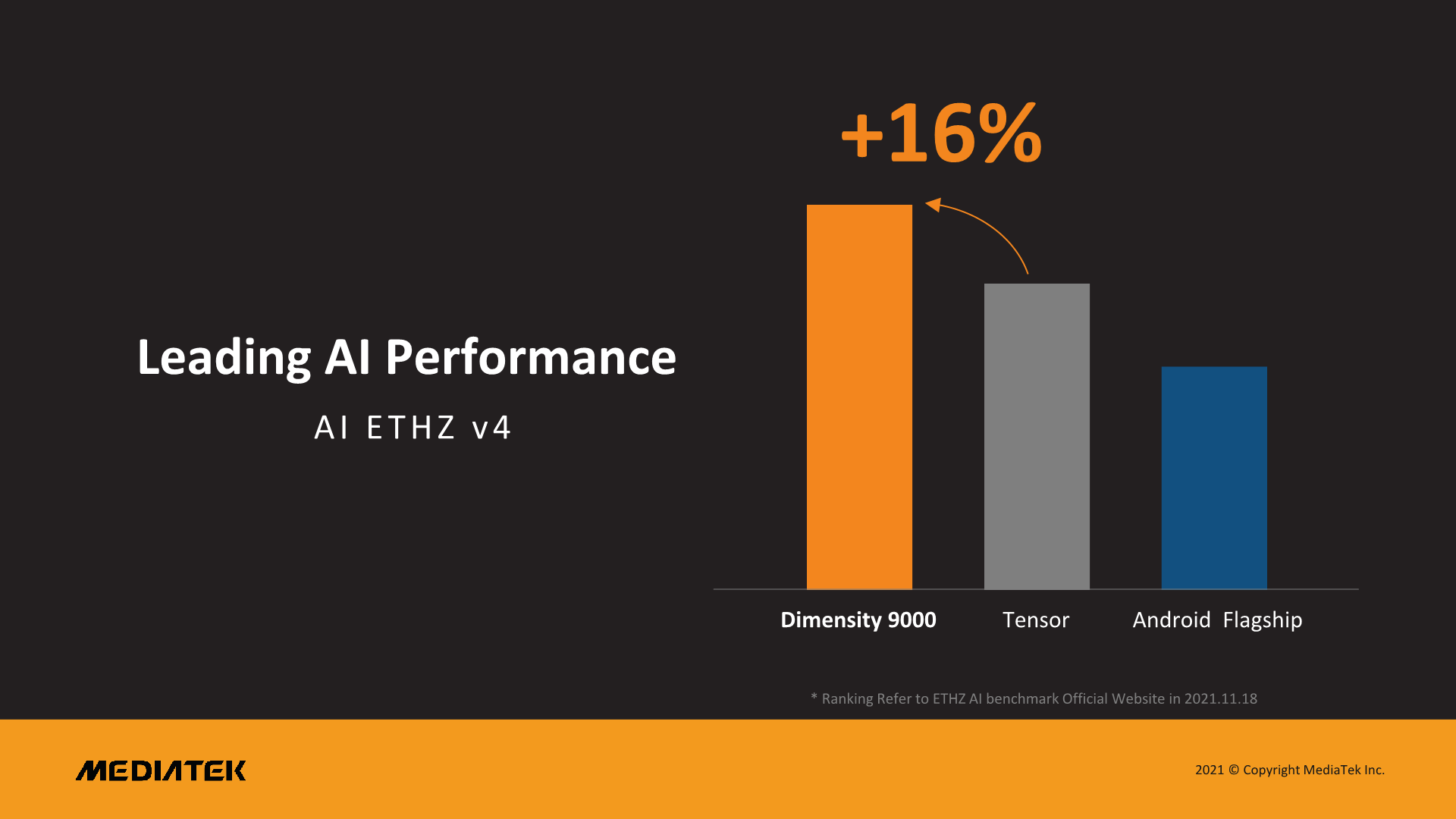
A more apples-to-apples comparison would be the ETHZ Ai Benchmark across Android devices, here the chip should take advantage of all accelerator blocks including CPU, GPU and NPU, and the Dimensity 9000 is advertised to beat the Google Pixel 6 and the Tensor SoC, which recently had notably outperformed the competition. MediaTek doing even better here seems to be promising for ML performance of the SoC. Naturally, we’ll have to see more detailed benchmarks for a more thorough analysis of the ML performance, but it seems MediaTek has developed a quite solid contender here.
Media Pipelines & Massive ISPs
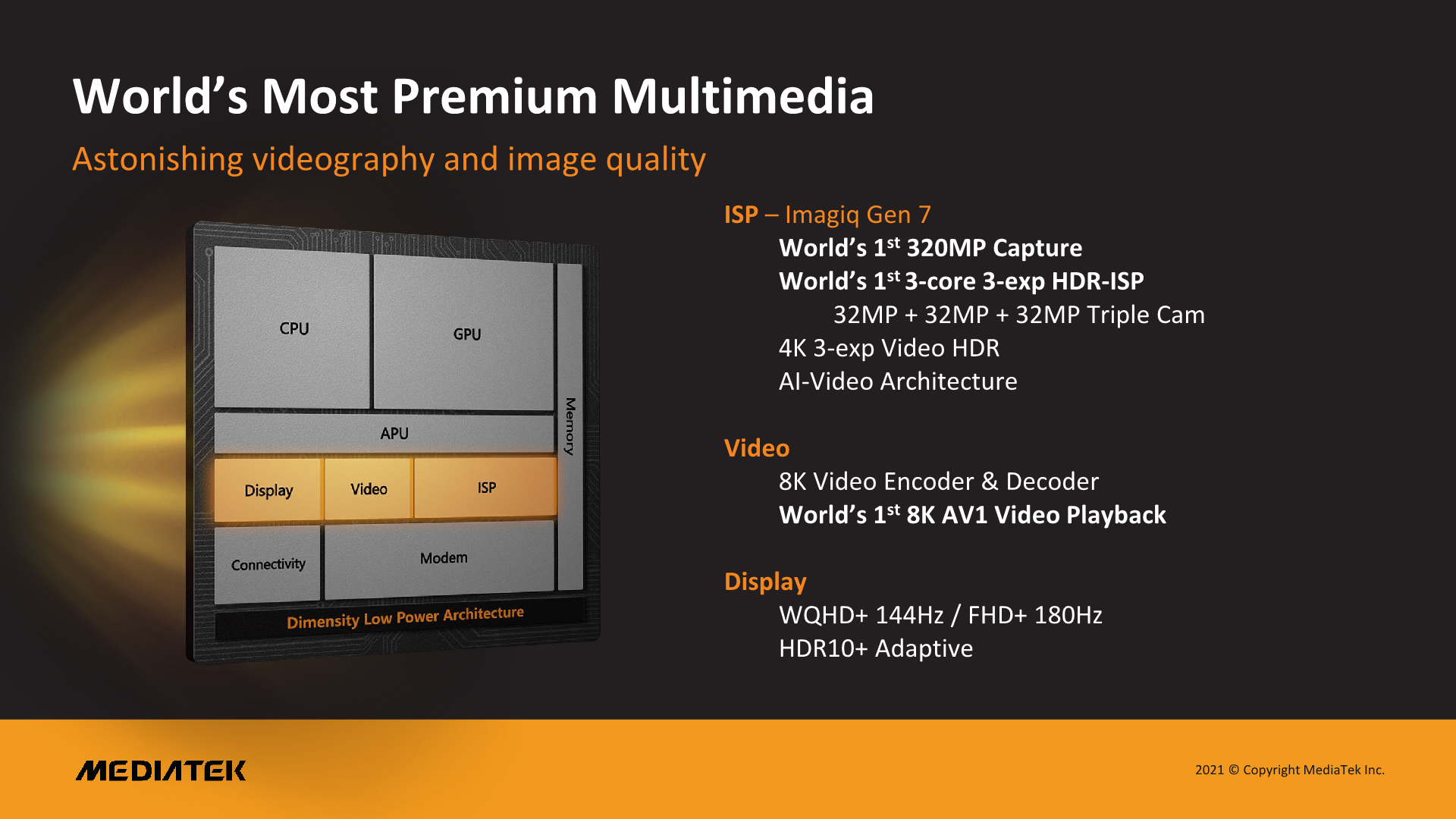
Moving onto the media side of things, MediaTek also throws in everything but the kitchen sink into the new SoC. We’ll get to the ISP in a bit, but in terms of video encoding and decoding, MediaTek supports all popular current codecs. There is no AV1 encoding yet, but the company says that the chip is the first in the industry to support 8K AV1 decoding – previous generation Dimensity and competitor SoCs only are able to do 4K decoding at the moment.
The display pipeline supports WQHD+ to 144Hz, or FHD+ to 180Hz with full HDR+ Adaptive (10-bit), so the chip should power the highest resolution and refresh rate screens out there.
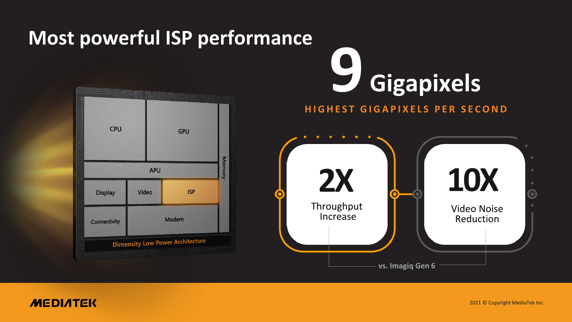
Getting back to the ISP, MediaTek claims that the camera subsystem is massively revamped in this generation. The Dimensity 9000 features triple ISPs with the ability for concurrent operation, with the chip being able to push through 9 Gigapixels/s. We’re not sure exactly if the figures are comparable across the vendor claims, but Qualcomm’s Snapdragon 888 “only” supports 2.7GPixel/s. Interestingly enough MediaTek says this is only a 2x throughput increase versus the Dimensity 1200.
The Imagiq790 ISP claims to be the world’s first to support 320MP sensors and MediaTek claims they’re working closely with the sensor vendors to enable such functionality. We’ve heard last year about 200MP sensors when Qualcomm announced the Snapdragon 888, and in September Samsung had announced the HP1 at this resolution, though we haven’t seen devices with it yet.
In triple-camera operation, the ISP supports concurrent 32+32+32MP sensor operation. We’ve seen such operation become more popular in sensor-fusion like scenarios for computation photography, or concurrent video recording on multiple sensors.
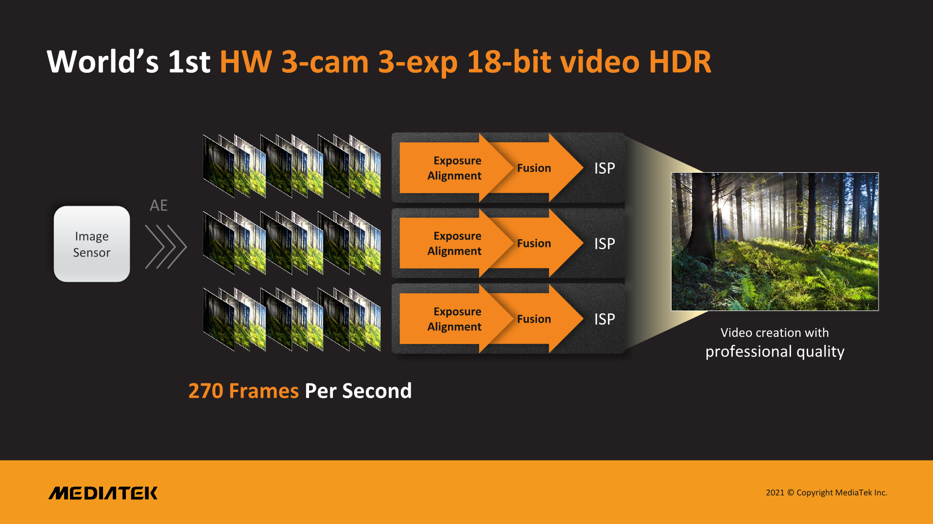
The new ISP also vastly improves its capabilities in terms of bit-depth, as MediaTek now upgrades it to a full 18-bit pipeline. Although mobile image sensors today natively are barely 10- or 12-bit at most in terms of their ADC bit-depth, multi-exposure image stacking has become the norm, especially with sensors now also getting more advanced HDR techniques such as staggered HDR captures. The new higher bit-depth ISP now is able to better do exposure merging across multiple frames, with the Dimensity 9000 able to do 270 frames per second (at presumably 4K resolution) across three sensors on its three ISPs.
The raw throughput and processing power here would be immense, and a massive leap over any other current SoC in the market.
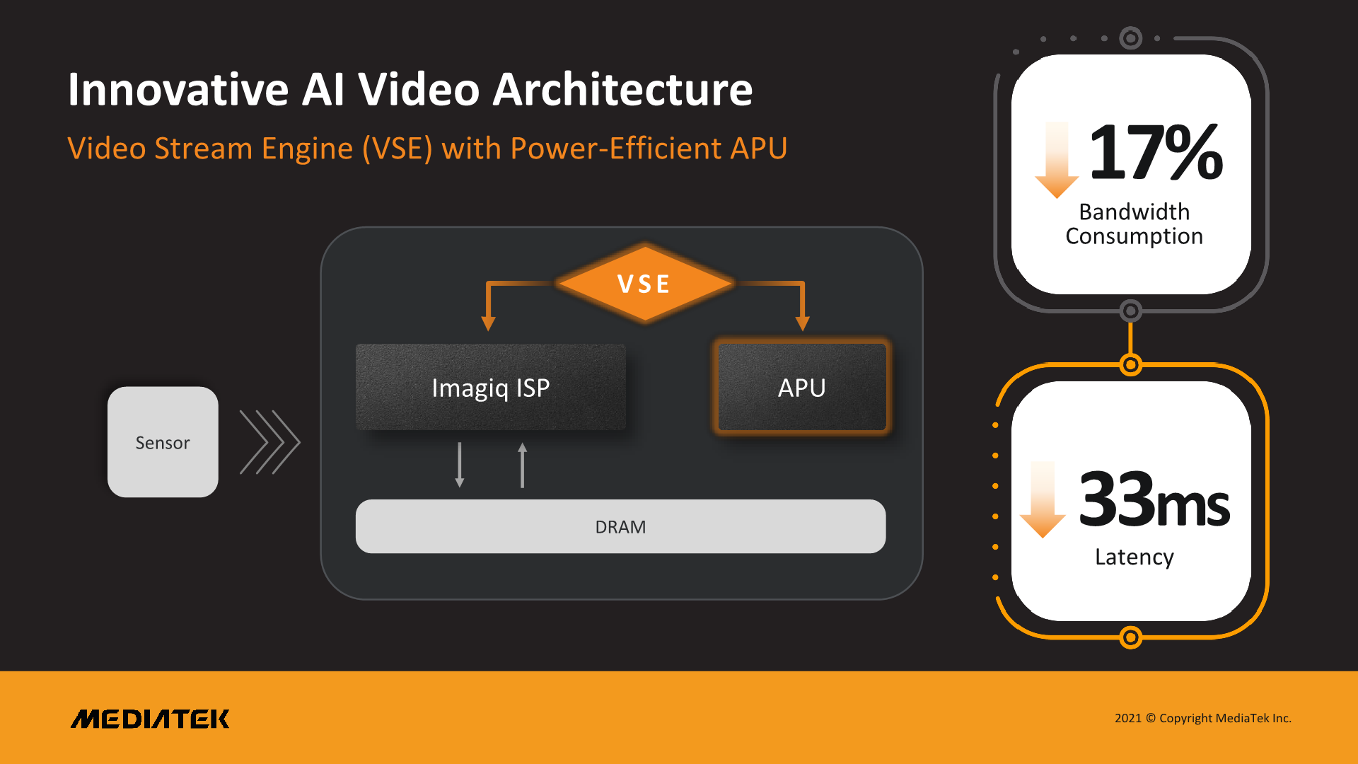
MediaTek says that they’ve improved the video pipelines as well, being able to tightly interact with the APU in a memory coherent fashion, bypassing the need to copy data over DRAM, increasing performance and decreasing bandwidth requirements and latency. Presumably vendors would be able to take advantage of the architecture to implement video recording with ML-based image processing models on-the-fly, essentially the same kind of technology Google had presented on its recent Pixel 6 phones and the Google Tensor chip.
Upgraded 5G Modem
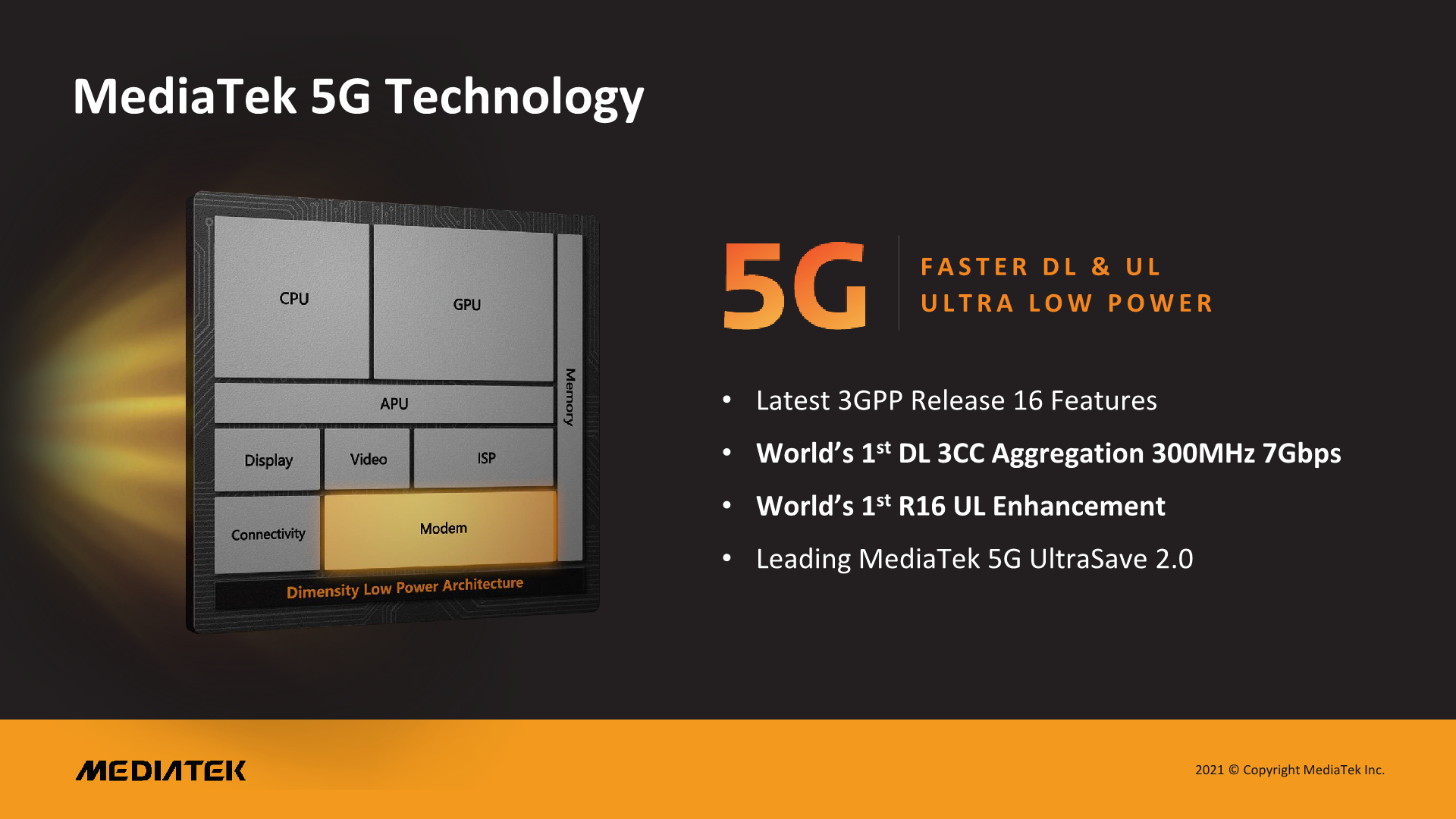
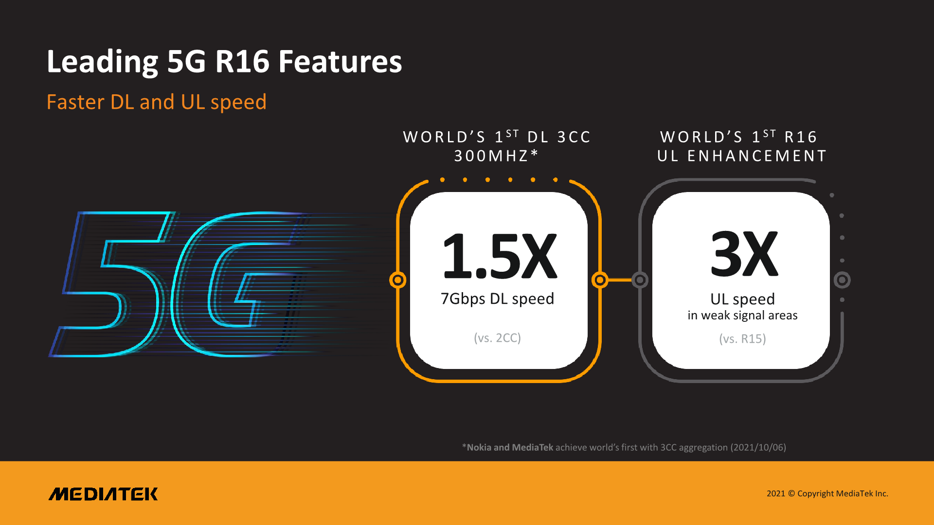
On the modem side, MediaTek has had quite a lot of success with its recent 5G modem implementations. The new Dimensity 9000 modem upgrades things even further, advertising for the first time 3CC carrier aggregation with up to 300MHz of Sub-6 bandwidth, allowing for download speeds of up to 7Gbps.
The modem is fully compatible with 3GPP release 16, with one larger change being UL Tx switching, which allows for better uplink capabilities and utilisation of spectrum in multi-band 5G NR deployments.
MediaTek notes that its modem has been extremely power efficient compared to competitor products, and the Dimensity 9000 will continue on this patch by providing advanced power saving technologies.
Although the modem features all the bells and whistles for Sub-6 5G, it does still lack mmWave. MediaTek notes that this is simply a result of the market need and the company’s current customer focus. Currently, the US remains the only market where mmWave truly remains a critical feature, as most vendors opt to not even equip their global device variants with mmWave modules. The company admits that due to this, we’ll unlikely see US devices powered by the Dimensity 9000, and the company is fine with that compromise, as it tries to cater to and focus on vendors which serve the rest of the world. MediaTek noted that next year, we will see mmWave product announcements for the US market, but these will at first be in the low/mid-range line-up.
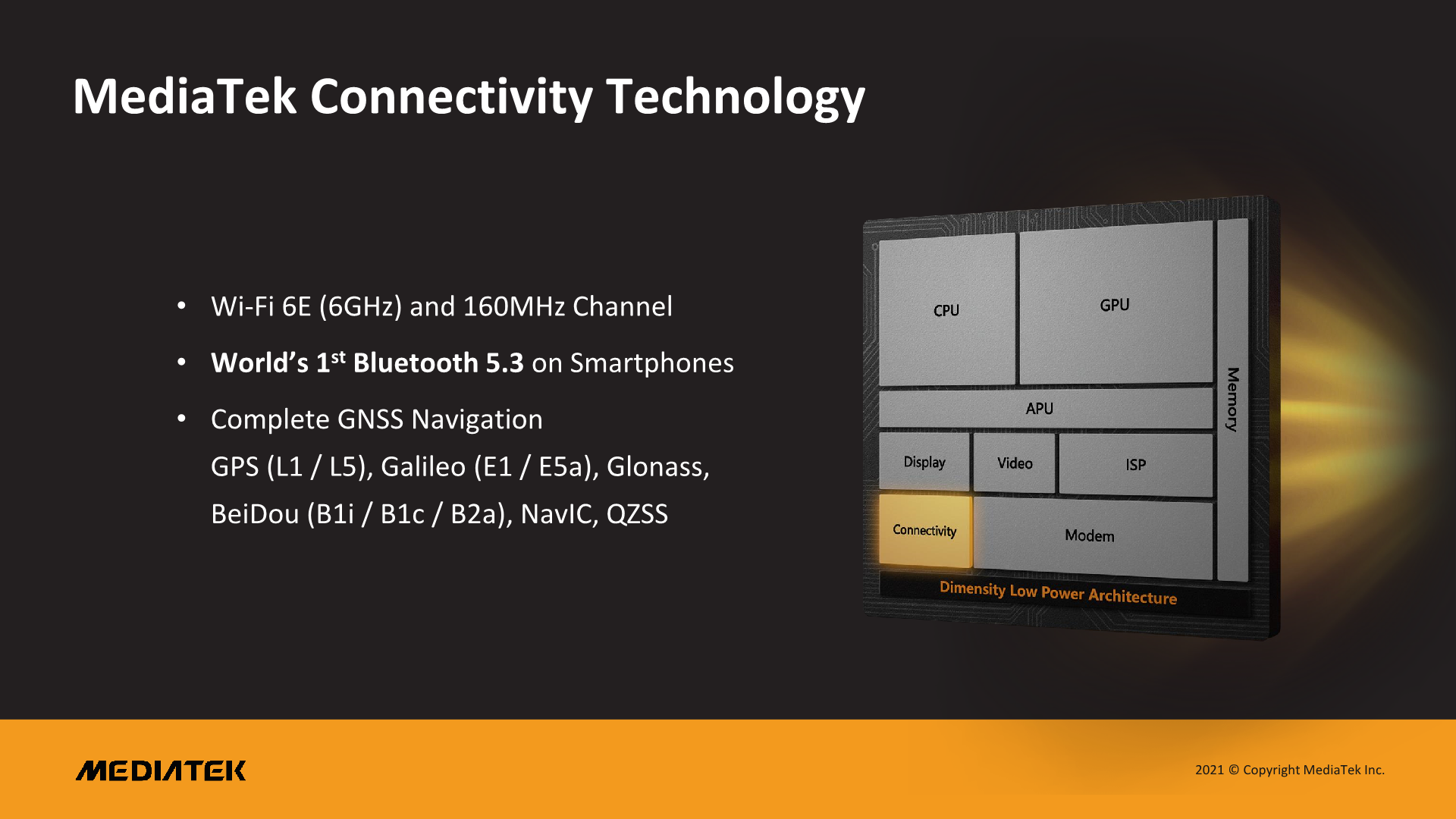
Finally, on the Wi-Fi side, MediaTek’s Dimensity 9000 platform also comes with their own in-house solution, now supporting Wi-Fi 6E for 6GHz band support, and 160MHz channel bandwidth, as well as Bluetooth 5.3. The GNSS solution now adds BDS-3 connectivity via B1C signals.


150 Comments
View All Comments
ChrisGX - Thursday, November 25, 2021 - link
The two statements that you take as contradicting one another are actually consistent - they refer to different matters. For an implementation of the G710 on the same silicon process as the predecessor G78 (TSMC N5) if power is held constant the Mali-G710 will offer a 20% performance improvement. However, the structure of the Mali cores change with the G710. You are only going to need roughly half of the number of cores to achieve equivalent performance to the earlier generation G78. The cores of the G710 are faster, bigger and more power hungry but in a sensible GPU configuration in an ARM SoC they offer a 20% energy efficiency boost in an ISO Process implementation.If the Dimensity 9000 is anything to go by it looks like ARM premium SoC manufacturers will be looking for big gains in GPU performance (much more than 20%) and they will be willing to pay a power consumption price to get it. So, with ARM SoCs in flagship Android phones already operating at the power limit for such devices power savings will have to be made elsewhere if sustainable performance is to see solid gains in 2022 phones.
tobichii6 - Friday, November 19, 2021 - link
I will not belive until they be friendly with open-source community as GNU GPL v2. Look at Qualcomm, they're still superior, of course their hardware decoder like AV1 Is I think still behind (update on me for this) but they can still whip your butt because of their soon snapdragon cpu. This is just talking of new architecture cpu meanwhile does not represent average software update, and plus it's a pain in the arse to mod a MediaTek device. And that's not funny at all. Because devices tend to go old, We need a source code so our devices would last long.
Change your policy about the source code to getting open then we're talking (all android chipset in mtk family must be open)
dwillmore - Friday, November 19, 2021 - link
Please don't use SLC for System Level Cache as SLC is already used for flash memories. It's going to cause confusion.FunBunny2 - Friday, November 19, 2021 - link
"SLC is already used for flash memories"SLC was used for flash memories
it's been a while since there was any SLC on sale anywhere.
Wereweeb - Friday, November 19, 2021 - link
There's plenty in servers, and almost all SSD's use their cells in pSLC mode for caching. The FuzeDrive uses it for tiering.mode_13h - Saturday, November 20, 2021 - link
I think it's the nomenclature ARM is using, though. It's reasonable to have a distinct term for cache that's shared among all the CPU cores *and* accelerator blocks, so I don't mind them not simply calling it L3 or LLC.Boss Win - Friday, November 19, 2021 - link
Too many Qualcomm employee attacking a chinese city taipei company MediaTek.Biggest excuse is communism stole tech. While capitalism stole Hawaii, California, New Mexico, and the whole USA.
And yeah, happy thanksgiving.. where people saved you from your winter deaths only to be killed by you after.
Stupid white men who want to rape 13 year old Pocahontas.
Raqia - Friday, November 19, 2021 - link
Their issue has always been software support which lags other vendors:https://www.androidauthority.com/qualcomm-mediatek...
Not to mention driver cheats. The part does look like the ARM presentation's '22 reference high end implementation and good on paper so hopefully it spurs more competition and innovation. HBM stacks on phones maybe? Split, mammoth sized CPU and GPU chiplets?
mode_13h - Saturday, November 20, 2021 - link
Cost is probably a big issue with both of those. We're likely to see stacked memory in laptops first (like what Apple did), before it ever reaches phones. I doubt if HBM can be power-efficient enough, which is probably why Apple went with LPDDR5, in the M1 Pro and Max.And a dedicated GPU chiplet in phones? Doesn't seem likely. Maybe if yields of even newer processes are poor.
wjohnas - Saturday, November 20, 2021 - link
Samsung's Exynows 2100 already supports 8K@60fps AV1 Decoding, I don't know what Mediatek talking about