MediaTek Announces Dimensity 9000: Supercharged Flagship SoC on 4nm
by Andrei Frumusanu on November 18, 2021 6:00 PM EST5th Generation APU/NPU, a Massive ISP, and New 5G & WiFi
APU/NPU AI/ML Upgrades
Moving away from CPU and GPU, we find MediaTek’s new “APU”, or AI Processing Unit, or rather NPU as we more generically tend to call it nowadays. MediaTek always had one of the earliest in-house implementations of such an IP, and the Dimensity 9000 now implements the 5th generation of such an IP.
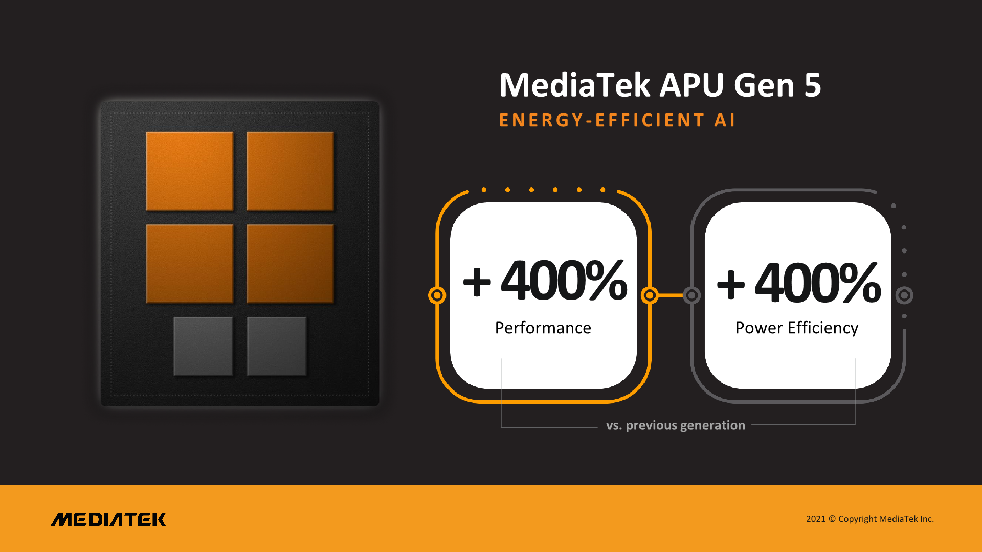
MediaTek promises a +400% performance and power efficiency improvement over the previous generation Dimensity 1200 implementation, which is quite a step-up, however should be contextualised to other more performant competitor platforms.
The company had made one slide available of showcasing MLPerf against Apple’s A15, noting +108% at +75% power efficiency versus the iPhone chip, the company here actually quoted our own published MLPerf figures, however we’ll avoid using the slide as the comparison isn’t great as the iOS variant of the app isn’t fully optimised and doesn’t take advantage of CoreML acceleration.
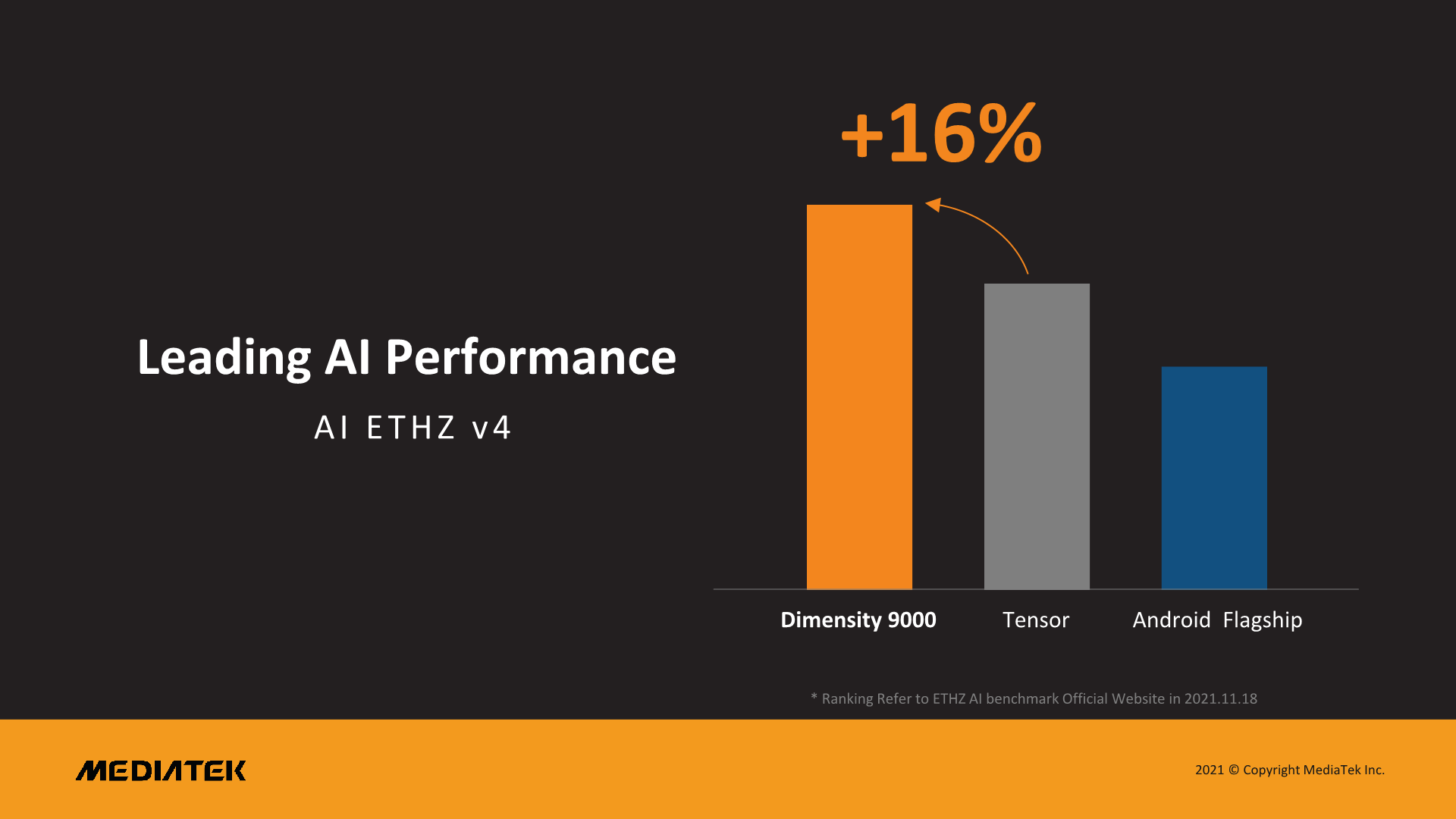
A more apples-to-apples comparison would be the ETHZ Ai Benchmark across Android devices, here the chip should take advantage of all accelerator blocks including CPU, GPU and NPU, and the Dimensity 9000 is advertised to beat the Google Pixel 6 and the Tensor SoC, which recently had notably outperformed the competition. MediaTek doing even better here seems to be promising for ML performance of the SoC. Naturally, we’ll have to see more detailed benchmarks for a more thorough analysis of the ML performance, but it seems MediaTek has developed a quite solid contender here.
Media Pipelines & Massive ISPs
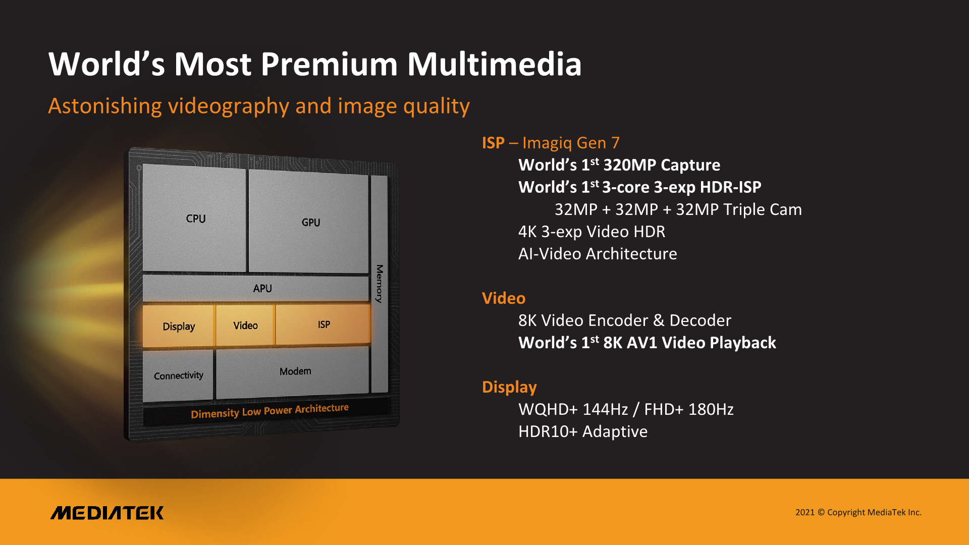
Moving onto the media side of things, MediaTek also throws in everything but the kitchen sink into the new SoC. We’ll get to the ISP in a bit, but in terms of video encoding and decoding, MediaTek supports all popular current codecs. There is no AV1 encoding yet, but the company says that the chip is the first in the industry to support 8K AV1 decoding – previous generation Dimensity and competitor SoCs only are able to do 4K decoding at the moment.
The display pipeline supports WQHD+ to 144Hz, or FHD+ to 180Hz with full HDR+ Adaptive (10-bit), so the chip should power the highest resolution and refresh rate screens out there.
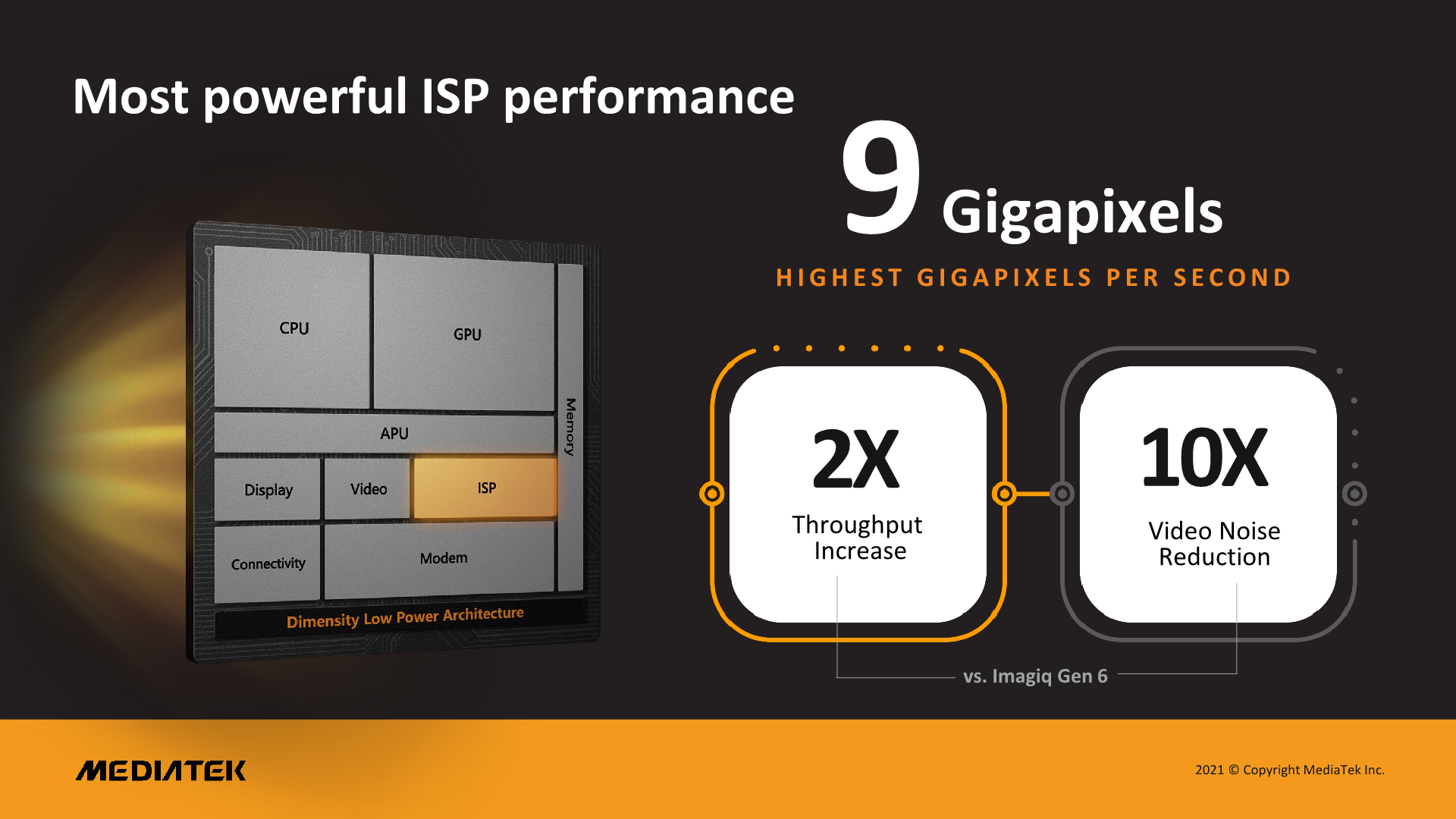
Getting back to the ISP, MediaTek claims that the camera subsystem is massively revamped in this generation. The Dimensity 9000 features triple ISPs with the ability for concurrent operation, with the chip being able to push through 9 Gigapixels/s. We’re not sure exactly if the figures are comparable across the vendor claims, but Qualcomm’s Snapdragon 888 “only” supports 2.7GPixel/s. Interestingly enough MediaTek says this is only a 2x throughput increase versus the Dimensity 1200.
The Imagiq790 ISP claims to be the world’s first to support 320MP sensors and MediaTek claims they’re working closely with the sensor vendors to enable such functionality. We’ve heard last year about 200MP sensors when Qualcomm announced the Snapdragon 888, and in September Samsung had announced the HP1 at this resolution, though we haven’t seen devices with it yet.
In triple-camera operation, the ISP supports concurrent 32+32+32MP sensor operation. We’ve seen such operation become more popular in sensor-fusion like scenarios for computation photography, or concurrent video recording on multiple sensors.
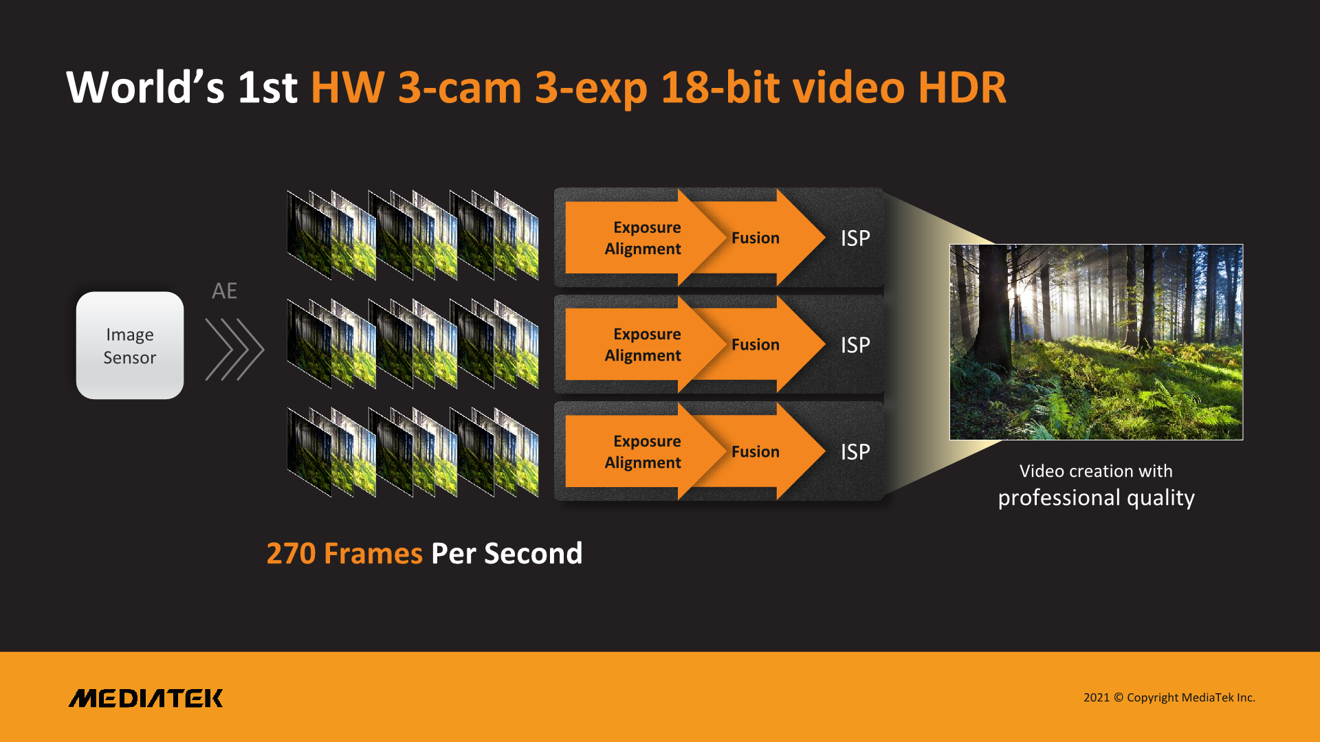
The new ISP also vastly improves its capabilities in terms of bit-depth, as MediaTek now upgrades it to a full 18-bit pipeline. Although mobile image sensors today natively are barely 10- or 12-bit at most in terms of their ADC bit-depth, multi-exposure image stacking has become the norm, especially with sensors now also getting more advanced HDR techniques such as staggered HDR captures. The new higher bit-depth ISP now is able to better do exposure merging across multiple frames, with the Dimensity 9000 able to do 270 frames per second (at presumably 4K resolution) across three sensors on its three ISPs.
The raw throughput and processing power here would be immense, and a massive leap over any other current SoC in the market.
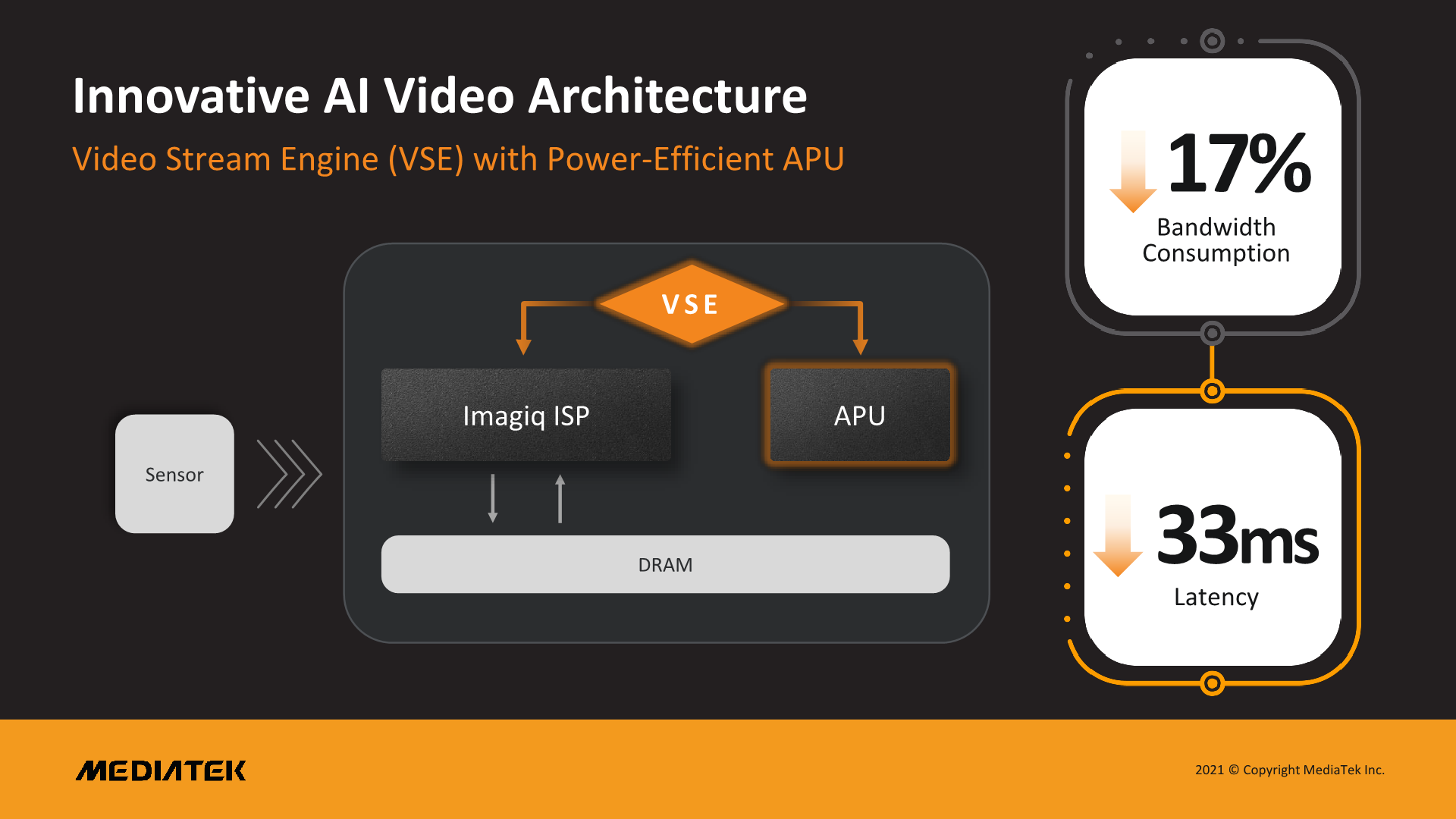
MediaTek says that they’ve improved the video pipelines as well, being able to tightly interact with the APU in a memory coherent fashion, bypassing the need to copy data over DRAM, increasing performance and decreasing bandwidth requirements and latency. Presumably vendors would be able to take advantage of the architecture to implement video recording with ML-based image processing models on-the-fly, essentially the same kind of technology Google had presented on its recent Pixel 6 phones and the Google Tensor chip.
Upgraded 5G Modem
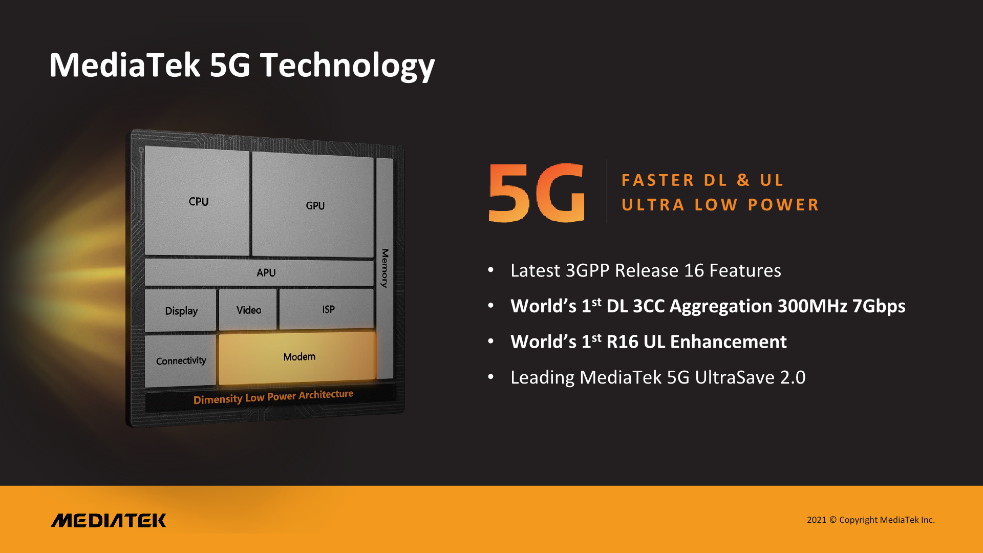
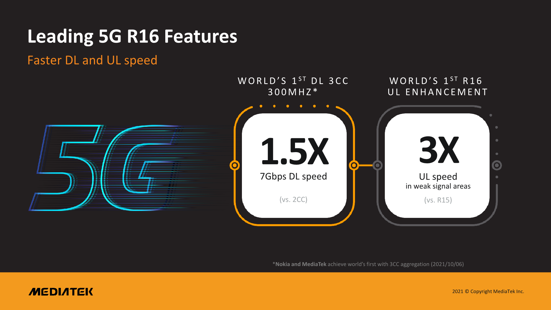
On the modem side, MediaTek has had quite a lot of success with its recent 5G modem implementations. The new Dimensity 9000 modem upgrades things even further, advertising for the first time 3CC carrier aggregation with up to 300MHz of Sub-6 bandwidth, allowing for download speeds of up to 7Gbps.
The modem is fully compatible with 3GPP release 16, with one larger change being UL Tx switching, which allows for better uplink capabilities and utilisation of spectrum in multi-band 5G NR deployments.
MediaTek notes that its modem has been extremely power efficient compared to competitor products, and the Dimensity 9000 will continue on this patch by providing advanced power saving technologies.
Although the modem features all the bells and whistles for Sub-6 5G, it does still lack mmWave. MediaTek notes that this is simply a result of the market need and the company’s current customer focus. Currently, the US remains the only market where mmWave truly remains a critical feature, as most vendors opt to not even equip their global device variants with mmWave modules. The company admits that due to this, we’ll unlikely see US devices powered by the Dimensity 9000, and the company is fine with that compromise, as it tries to cater to and focus on vendors which serve the rest of the world. MediaTek noted that next year, we will see mmWave product announcements for the US market, but these will at first be in the low/mid-range line-up.
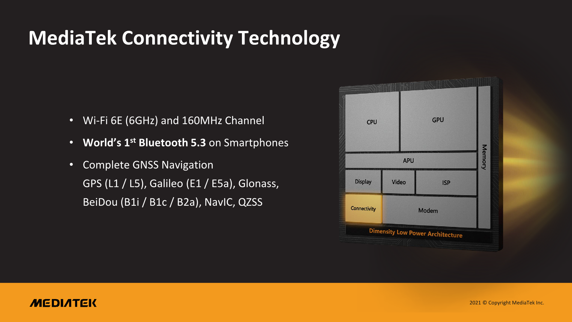
Finally, on the Wi-Fi side, MediaTek’s Dimensity 9000 platform also comes with their own in-house solution, now supporting Wi-Fi 6E for 6GHz band support, and 160MHz channel bandwidth, as well as Bluetooth 5.3. The GNSS solution now adds BDS-3 connectivity via B1C signals.


150 Comments
View All Comments
UNLK A6 - Tuesday, November 23, 2021 - link
To see the original slides, they're still at 9to5google.com. Search for "Dimensity 9000".UNLK A6 - Tuesday, November 23, 2021 - link
...And notice they credit AnandTech for those images. What the heck AnandTech, how about a remark someplace that you changed the article!Frenetic Pony - Thursday, November 18, 2021 - link
Damn, that entire camera isp section was about as useless as most camera numbers are in phones these days. "200mp, 18bit, 200 gigapixels-" shut up, your tech is wasted, why are you advertising it to people that should know better?arayoflight - Friday, November 19, 2021 - link
200MP capture pipeline also means that you can do 17 frames of 12MP for better HDR stacking and merging.A more competent ISP benefits even lower resolution sensors.
Also simultaneous capture of multiple 4k streams is great as it will allow for smooth switching of cameras during capture. Currently only iPhone can do that.
hanselltc - Friday, November 19, 2021 - link
Nice claims and nice specs, but we'll have to see where they end up and how they actually perform.The D1000-1200 chips also had rather nice specs, but other than Nord 2 they were basically china exclusives.
On the A15 review's performance/energy chart D1200 basically got bodied by 865, and then there's apple doing 3 quarters of its middle core's performance on blizzards with half energy.
Huawei cranked Kirin 9000 out with Arm Holdings IP for the CPU/GPU and had them actually trashing everything android while going at apple for GPU. A year later this thing calls itself 9000 again, lets see if it performs.
dotjaz - Friday, November 19, 2021 - link
That's definitely not how it works. The pipeline is 9GPix/s. It has nothing to do with the maximum resolution. That 320MP is likely not zero-lag and lacking a lot of processing. That's why triple camera only have less than 1/3 the total pixel counts.eastcoast_pete - Thursday, November 18, 2021 - link
On another note, Samsung's fabs better have an answer for this N4 node from TSMC soon, or Qualcomm might rethink their choice of foundry quite quickly. Plus, NVIDIA isn't too pleased with the efficiency (lack thereof) of Samsung's N8 process. But for now, both QC and NVIDIA might be stuck with Samsung, as TSMC seems to be quite booked for now, and not just on their advanced EUV (N5, N4) nodes.dotjaz - Friday, November 19, 2021 - link
Nvidia chose an old node that was never claimed to be as efficient. Why would Nvidia blame Samsung for it?You don't even know the actual name of the node, it's 8N. So I suggest you shut up until you get your facts right.
Kangal - Friday, November 19, 2021 - link
Excluding the questionable SMIC offerings, Samsung actually proposes the best performance per dollar lithography. And they deliver too.TSMC is pricey stuff. Part of that is the stable revenue stream that came from AMD and the consoles, allowing them to expand their R&D budget.
The truth is, the Kirin 9000 doesn't matter, and neither does the Dimensity 9000. They hardly ever make any supplies of it. I'd rather a "Good SoC" working on my phone, rather than a "Great SoC" which is almost vaporware/paper-launch.
vladx - Saturday, November 20, 2021 - link
Vaporware my ass, here writing to you from a Mate 40 running on a Kirin 9000E. People here in EU are not brainwashed to get our phones straight from carriers, we can actually think for ourselves and buy from stores which doesn't limit your options to a couple of phone models only.