MediaTek Announces Dimensity 9000: Supercharged Flagship SoC on 4nm
by Andrei Frumusanu on November 18, 2021 6:00 PM EST
MediaTek over the last few years has generally always been regarded as the “other” SoC vendor in the mobile industry, with most media and consumer attention being paid to the flagship SoC products by the likes of Apple, Qualcomm, Samsung and HiSilicon. Indeed, the last time MediaTek had attempted a true flagship SoC was several years ago with the Helio X20 and X30, before seeing very little success in the market and instead refocusing on the mid-range and “premium” segments.
Today, MediaTek is looking to change this positioning. After seeing new-found success in the market, particularly seeing a fantastic 2020 and 2021, where the Taiwanese vendor is now able to claim the #1 spot with 40% market share, as well as a growing 28% of 5G SoC market share, the company is now also aiming for recognition and leadership position in the flagship SoC market – this is where the new Dimensity 9000 comes in.
The Dimensity 9000 is MediaTek’s latest effort in creating a no-compromise flagship SoC, with the designers throwing in everything but the kitchen sink at it in terms of specifications, representing a lot of industry firsts, such as the first Armv9 SoC with Cortex-X2, A710’s and A510’s CPUs, a new Mali-G710 GPU, first LPDDR5X compatible SoC, astounding camera ISP claims, and the first outright publicly announced TSMC N4 silicon design in the industry. The list of features and capabilities is extensive, and the announcement today definitely represents MediaTek’s largest effort in generations and years.
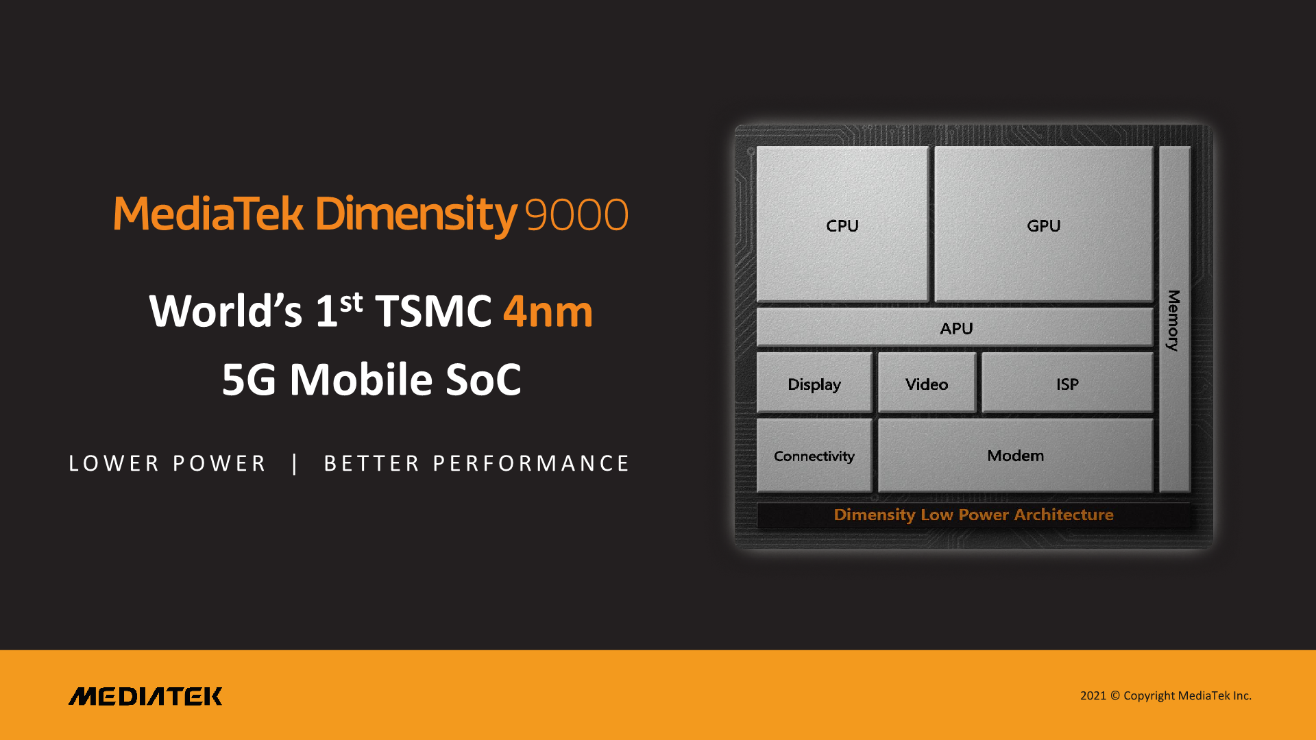
Starting off with the process node, MediaTek is able to claim a first in the industry, with the Dimensity 9000 being the world’s first TSMC N4 chip. Over the past few years, we’ve always been accustomed that either Apple or HiSilicon be the very first customers on TSMC’s latest leading-edge nodes. With HiSilicon being cut-off from TSMC, that left Apple as the obvious lead partner for TSMC’s new generation process nodes – however, the timing here just didn’t work out for the A15 as the N4 node just wasn’t ready yet. With Qualcomm currently being tied to Samsung Foundry for their flagships (arguably with not great success), this left a vacuum for where HiSilicon used to be, which MediaTek is now looking to fill. In fact, I think this would be the company’s first time where they’re truly on a leading edge node since the 20nm days.
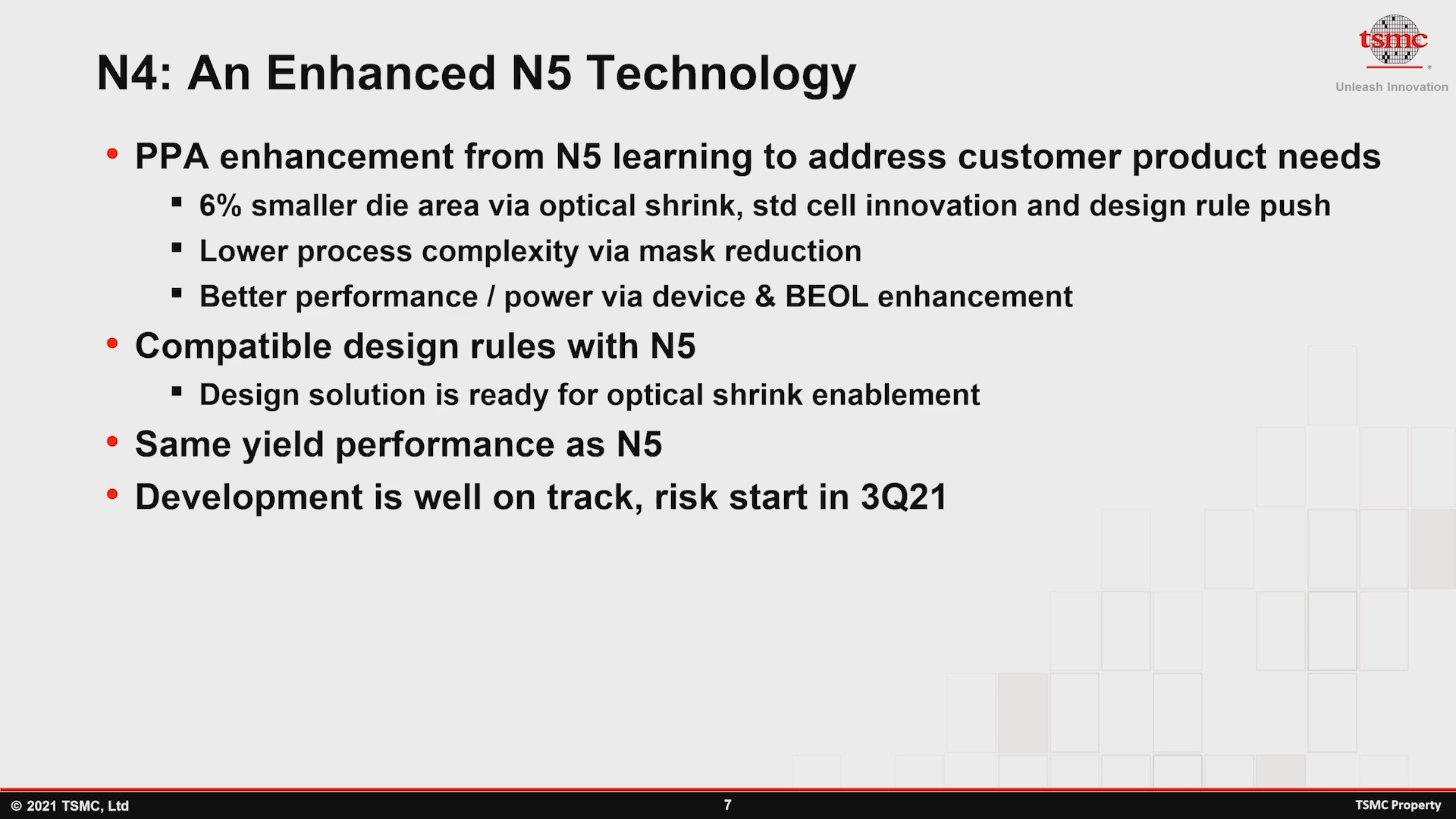
TSMC’s N4 node is supposed to be a smaller optical shrink over the N5 node, resulting in 6% more density, with similar single-digit improvements in performance and efficiency. TSMC had announced risk production for N4 to start in 3Q21, and with the Dimensity 9000 planned to hit commercial devices in 1Q22, the chip is likely the lead product for the process node.
| New MediaTek Flagship SoC 2022 | |
| SoC |
Dimensity 9000 |
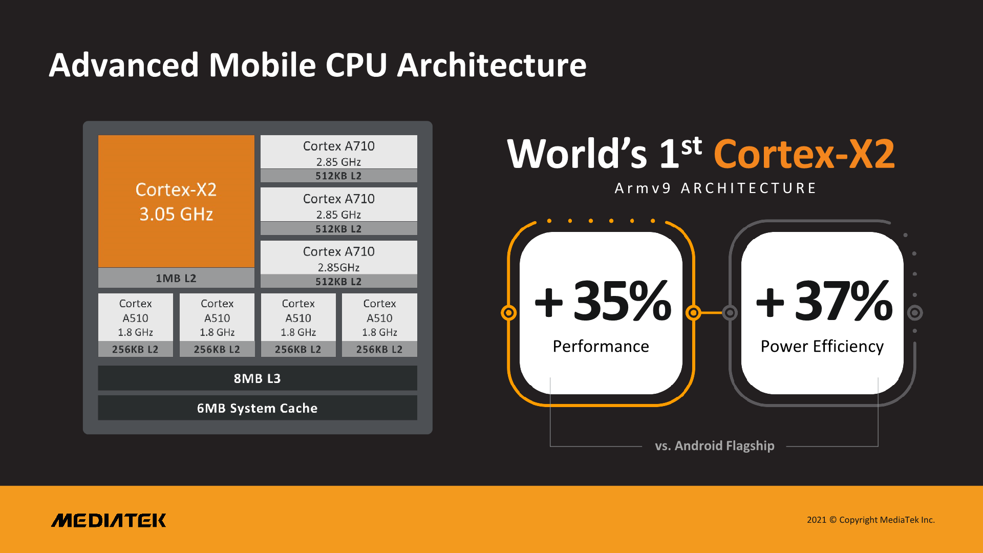
| CPU | 1x Cortex-X2 @ 3.05GHz 1x1024KB pL2 3x Cortex-A710 @ 2.85GHz 3x512KB pL2 4x Cortex-A510 @ 1.80GHz 4x256KB pL2 8MB sL3 |
| GPU | Mali-G710MP10 @ ~850MHz |
| Memory Controller |
4x 16-bit CH @ 3200MHz LPDDR5 / 51.2GB/s @ 3750MHz LPDDR5X / 60.0GB/s 6MB System Cache |
| ISP | Imagiq790 New-gen Triple 18-bit ISP 9GPix/s processing throughput Single Sensor up to 320MP Triple Sensor 32+32+32MP |
| NPU | 5th Gen 4+2 core APU |
| Media | 8K30 & 4K120 encode & 8K60 decode H.265/HEVC, H.264, VP9 8K30 AV1 Decode |
| Modem | (LTE Category 24/18) (5G NR Sub-6) |
| Mfc. Process | TSMC N4 |
There’s a lot to talk about the Dimensity 9000, so obviously enough as MediaTek advertises it as the first Armv9 SoC, let’s start off with the CPU configuration and the various IPs employed here.
No-Compromise CPU Setup
Being an Armv9 SoC, this means that the company is refreshing all the CPU IPs, employing the new Cortex-X2, Cortex-A710, and Cortex-A510 IPs from Arm. We had covered the new generation CPUs extensive earlier this year, so be sure to read up on those articles.
The Dimensity 9000 goes with a 1+3+4 CPU setup that has seen popularity in the market ever since Qualcomm had adopted the setup for the first time in the Snapdragon 855. For the performance cores, MediaTek uses the new Cortex-X2 cores, equipping them with the full 1MB of L2 cache, and clocking them at up to 3.05GHz. The clock frequency is higher than what we’re seeing from designs today on X1 cores such as the Snapdragon 888 or the Exynos 2100 at respectively 2.86 and 2.9GHz, but those competing SoCs were also on an inferior Samsung 5LPE process node. We don’t yet know exactly where the next-gen Snapdragon and Exynos chips will end up in terms of clocks, but I think it’s unlikely they will exceed the 3GHz mark, leaving the new Dimensity 9000 with a likely frequency advantage, and thus also a likely single-threaded performance leadership position amongst the Android SoC vendors.
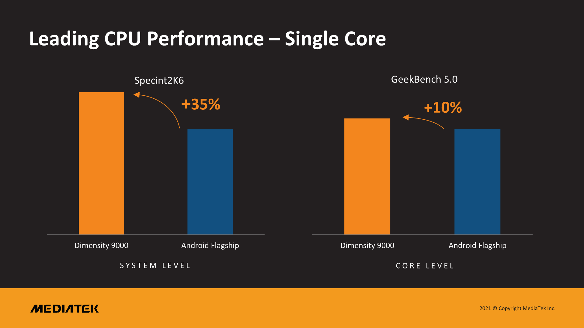
MediaTek does quote a +35% performance leap over current generation Android Flagship chips, which we assume is going to be a Snapdragon 888, however also states that efficiency is +37% better. This would mean that peak absolute power levels for the MediaTek 9000’s X2 cores would be similar to what we’re seeing from the X1 cores in a Snapdragon 888 today, which generally is a good position to be in, and the figures generally line up with what we expect from the IPC and process node differences between the designs.
MediaTek did note that the performance leap in more memory-bound workloads to be much higher than more core-local workloads, for example SPECint2006 seeing a +35% increase, while GeekBench 5 only will see a +10.5% increase over the competition. This generally also lines up with our understanding of the Cortex-X2, pointing out to low IPC improvements in anything that’s not taking advantage of the increase caches of the CPU cluster.
The middle cores of the Dimensity 9000 are 3x Cortex-A710 cores, equipped with 512KB L2’s, and clocked up to 2.85GHz. In this regard, MediaTek’s approach here is more similar to the Exynos 2100 in that it’s using quite high frequency mid-cores, in contrast to the lower 2.4GHz design point Qualcomm employs.
Alongside the middle cores, we also see the new Cortex-A510 little cores, and here MediaTek is doing things quite differently compared to what we expected from the first iterations of the IP. Instead of using Arm’s new “merged-core” approach, where a Cortex-A510 complex can consist of two cores sharing a SIMD/FP pipeline as well as a shared L2, MediaTek completely ignores this design aspect of the IP and instead goes the traditional route of only using one core per complex, with each core thus having its own SIMD/FP pipeline and private L2 cache. The cache here lies in at 256KB, which is also quite large, and short of the 512KB maximum. In effect, what MediaTek has done here is to configure the A510 cores with a near-maximum performance setup. While we still have our reservations about the cores, it’s good to see MediaTek not skimping out on the new designs.
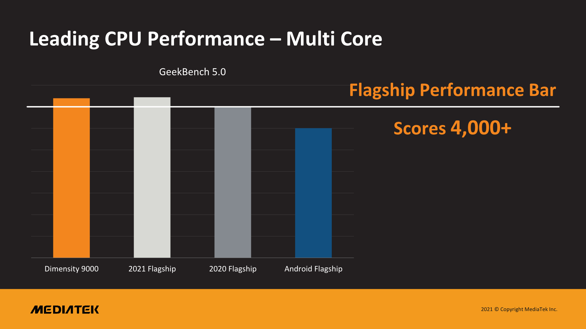
Due to the strongly configured middle cores, as well as well equipped little cores, the multi-core performance of the Dimensity 9000 is advertised as well exceeding the current Android competition, and falling in line with Apple achieves on the A15.
At the cluster level, MediaTek also equips the DSU with 8MB of L3 – this is likely the new generation DSU-110 as well.
On the CPU side, the Dimensity 9000 is essentially configured in the most optimal way – MediaTek went all-out in terms of frequencies and caches, and it’s generally hard to imagine a more performant configuration than what the chip is currently set up with, at least in the context of Arm Cortex CPU IP.
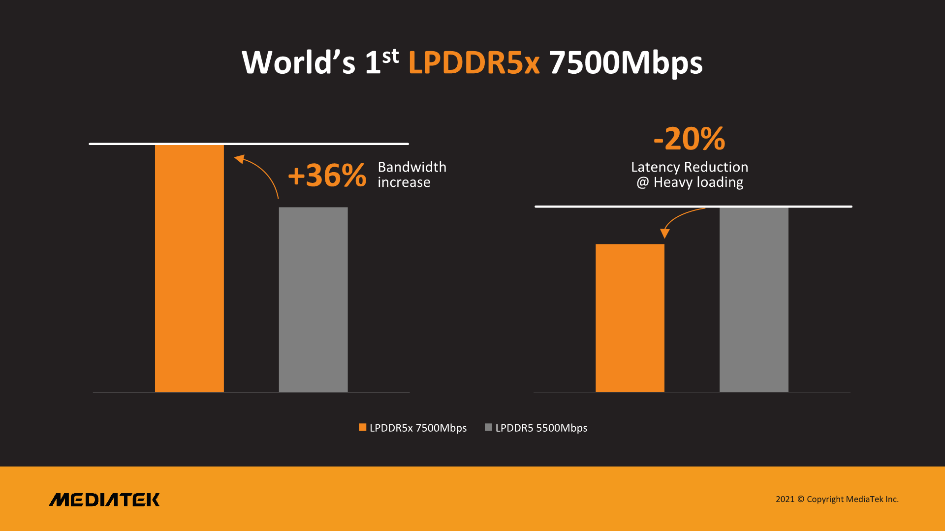
First LPDDR5X, Large System Cache
Another world first for the Dimensity 9000 is the fact that it’s the first chip announced to be compatible with LPDDR5X. The standard had only been published by JEDEC in July of this year, so the fact that the chip already supports it means that MediaTek was working off a draft and should be fully compatible with the new standard. While the full standard is advertised to go up to 8533Mbps support, the chip here does limit itself to 7500Mbps, so that means +17% bandwidth compared to current generation LPDDR5-6400 solutions. Still, I hadn’t expected LP5X SoCs until next late next year, so this was definitely a surprise. Naturally, the memory controller still fully supports LPDDR5 at up to 6400Mbps in case a vendor chooses to employ different memory modules.
The Dimensity 9000 is MediaTek’s first SoC also employing a system cache at 6MB. During the briefing, MediaTek noted that larger caches and SoC designs with system caches are definitely the way forward and is where everybody will be aiming for in the future. System level caches, or how we like to call them abbreviated, SLCs, are able to amplify performance of SoC blocks other than just the CPU, as well as reduce the memory traffic to DRAM, also having a positive benefit to power efficiency.
GPU: Mali G710MP10
On the GPU side of things, the MediaTek Dimensity 9000 is also the first SoC to see the deployment of the new Mali-G710 GPU. Earlier this year when we talked about the IP we had mentioned that MediaTek was the only remaining vendor that was expected to release an SoC with a larger Mali GPU implementation, given HiSilicon’s troubles and Samsung’s adoption of AMD RDNA GPUs.
The configuration on the Dimensity 9000 is a 10-core. We have to remember here that in terms of per-core performance one new G710 core is roughly equivalent to two G78 cores, so in terms of size and performance the new chip’s GPU is roughly comparable to the Google Tensor G78MP20 GPU, plus maybe an expected 20% performance boost due to generational IP improvements. MediaTek noted the peak frequencies to be at around 850MHz (exact clock to be confirmed).
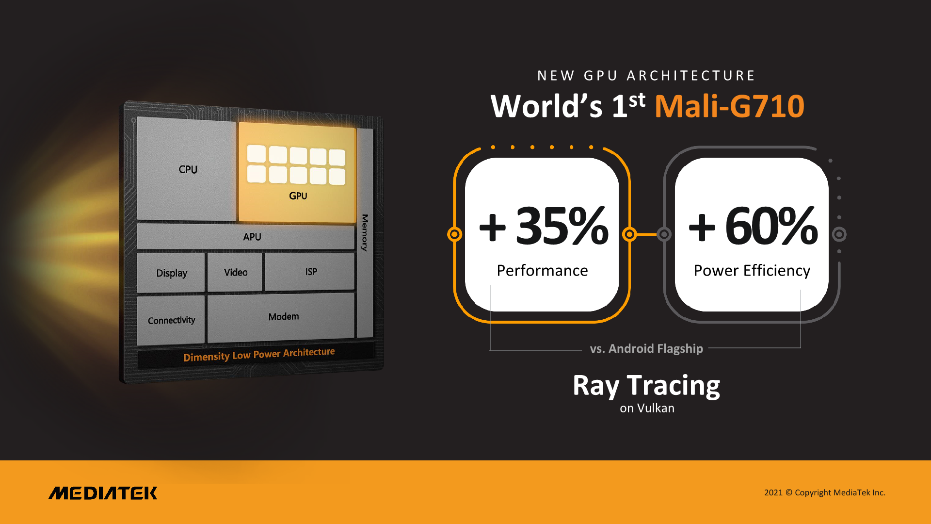
In terms of performance figures, the company’s materials advertised +35% vs the current Android flagships, while efficiency being +60% better. All of this year’s flagships had been rather disappointing in gaming efficiency, and we saw absolute power figures reaching +7.5-9W on the leading Exynos, Tensor and Snapdragon chips. MediaTek noting that their efficiency advantage is significantly larger than their performance leap also suggests they’re using lower peak power levels that what we see today, which is definitely a welcome change.
The company makes note of Ray Tracing capability, but this is simply a software API implementation rather than hardware, as the G710 doesn’t yet support this.
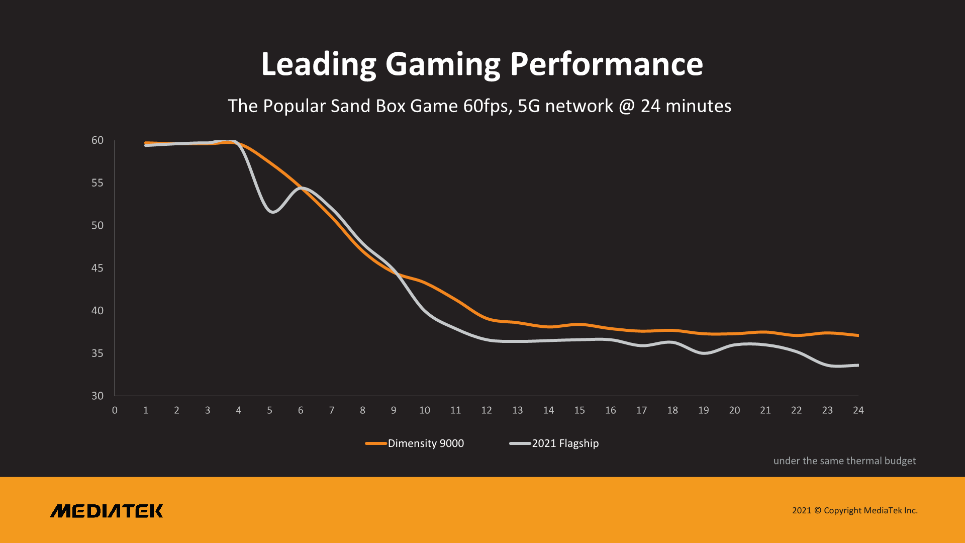
MediaTek had a slide showcasing longer term performance versus an iPhone 13 with the A15, with the Dimensity 9000 being able to slightly exceed the performance of the iPhone. We saw that the new iPhones throttle to around 3-3.5W, and that under cellular conditions the phones are reported to perform even worse due to the bad thermals. MediaTek notes the comparison is made under a similar thermal budget, so hopefully the comparison is valid here. It's to be noted, as we wrote in our A15 review, comparing real-world games such as Genshin Impact for GPU analysis isn’t great as the game always runs at different internal resolutions or detail levels, especially between Android and iOS.
That being said, MediaTek’s efficiency claims for the GPU do position it extremely well, and would likely allow it to effectively compete against the upcoming Snapdragon and Exynos chips which are still projected to arrive on less efficient process nodes.
Low-Power Leadership Claims
An interesting claim from MediaTek is that they are achieving low power leadership, thanks to the new TSMC N4 node as well as the smart power management the SoC as well as the platform is designed with.
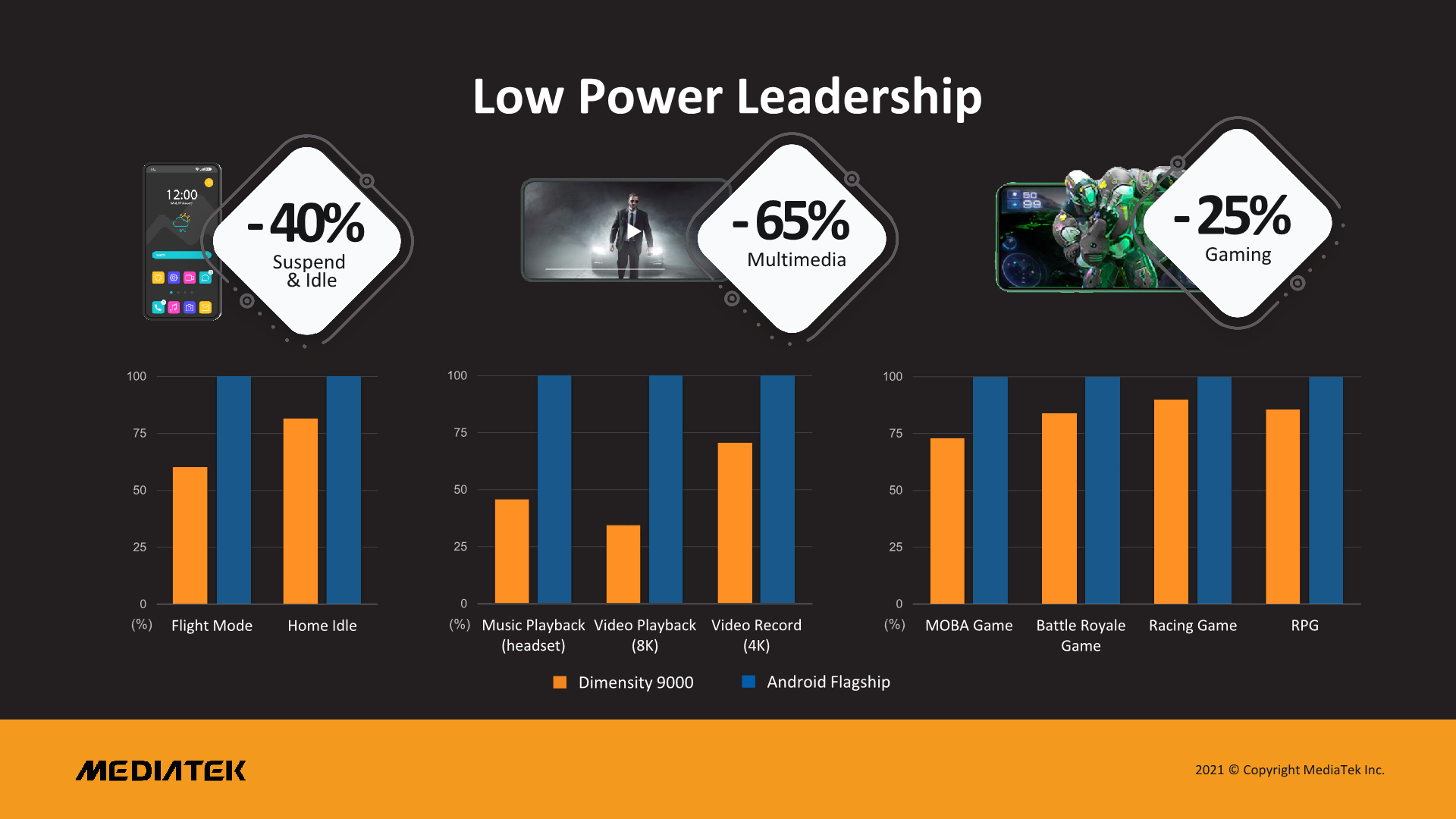
The above figures are comparisons of platforms total power, excluding power supply towards the display panel. This means we’re seeing a power comparison of the SoC, DRAM, PMICs, cellular RF and Wi-Fi systems – essentially the “platform” components which the SoC vendors are generally responsive for and which they bundle their offerings with.
Notable figures here are the media playback and recording numbers, where the Dimensity 9000 is said to have much lower power consumption than the competition. Gaming power is also said to be lower, but this is to be expected given the GPU efficiency and lower power claims.
The one data-point I find most interesting is the home idle power. One of the hardest things to achieve in a silicon design is doing nothing in an efficient manner, this actually represents a large percentage of energy consumption and affects the baseline power of a device, and thus your every-day battery life. Getting -20% over the competition here is quite respectable.


150 Comments
View All Comments
UNLK A6 - Tuesday, November 23, 2021 - link
To see the original slides, they're still at 9to5google.com. Search for "Dimensity 9000".UNLK A6 - Tuesday, November 23, 2021 - link
...And notice they credit AnandTech for those images. What the heck AnandTech, how about a remark someplace that you changed the article!Frenetic Pony - Thursday, November 18, 2021 - link
Damn, that entire camera isp section was about as useless as most camera numbers are in phones these days. "200mp, 18bit, 200 gigapixels-" shut up, your tech is wasted, why are you advertising it to people that should know better?arayoflight - Friday, November 19, 2021 - link
200MP capture pipeline also means that you can do 17 frames of 12MP for better HDR stacking and merging.A more competent ISP benefits even lower resolution sensors.
Also simultaneous capture of multiple 4k streams is great as it will allow for smooth switching of cameras during capture. Currently only iPhone can do that.
hanselltc - Friday, November 19, 2021 - link
Nice claims and nice specs, but we'll have to see where they end up and how they actually perform.The D1000-1200 chips also had rather nice specs, but other than Nord 2 they were basically china exclusives.
On the A15 review's performance/energy chart D1200 basically got bodied by 865, and then there's apple doing 3 quarters of its middle core's performance on blizzards with half energy.
Huawei cranked Kirin 9000 out with Arm Holdings IP for the CPU/GPU and had them actually trashing everything android while going at apple for GPU. A year later this thing calls itself 9000 again, lets see if it performs.
dotjaz - Friday, November 19, 2021 - link
That's definitely not how it works. The pipeline is 9GPix/s. It has nothing to do with the maximum resolution. That 320MP is likely not zero-lag and lacking a lot of processing. That's why triple camera only have less than 1/3 the total pixel counts.eastcoast_pete - Thursday, November 18, 2021 - link
On another note, Samsung's fabs better have an answer for this N4 node from TSMC soon, or Qualcomm might rethink their choice of foundry quite quickly. Plus, NVIDIA isn't too pleased with the efficiency (lack thereof) of Samsung's N8 process. But for now, both QC and NVIDIA might be stuck with Samsung, as TSMC seems to be quite booked for now, and not just on their advanced EUV (N5, N4) nodes.dotjaz - Friday, November 19, 2021 - link
Nvidia chose an old node that was never claimed to be as efficient. Why would Nvidia blame Samsung for it?You don't even know the actual name of the node, it's 8N. So I suggest you shut up until you get your facts right.
Kangal - Friday, November 19, 2021 - link
Excluding the questionable SMIC offerings, Samsung actually proposes the best performance per dollar lithography. And they deliver too.TSMC is pricey stuff. Part of that is the stable revenue stream that came from AMD and the consoles, allowing them to expand their R&D budget.
The truth is, the Kirin 9000 doesn't matter, and neither does the Dimensity 9000. They hardly ever make any supplies of it. I'd rather a "Good SoC" working on my phone, rather than a "Great SoC" which is almost vaporware/paper-launch.
vladx - Saturday, November 20, 2021 - link
Vaporware my ass, here writing to you from a Mate 40 running on a Kirin 9000E. People here in EU are not brainwashed to get our phones straight from carriers, we can actually think for ourselves and buy from stores which doesn't limit your options to a couple of phone models only.