Intel Architecture Day 2021: A Sneak Peek At The Xe-HPG GPU Architecture
by Ryan Smith on August 19, 2021 9:00 AM EST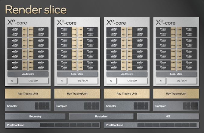
For Intel’s 2021 Architecture Day presentations, the yin to the CPU company’s traditional yang is GPUs. Intel has spent the last few years preparing to enter the market for discrete GPUs, with aims of competing in everything from consumer video cards up to HPC-class accelerators. And now, as the company already begins preparing for 2022, those efforts are finally coming to a head. Intel’s big breakout effort in the discrete GPU space starts in earnest next year with Xe-HPG and Xe-HPC, so for their 2021 architecture day, Intel is opening up a bit more about the GPU architectures that will be driving their first wave of high-performance products next year.
Between Xe-HP, Xe-HPC, and Xe-HPG, Intel has a very full plate of GPU designs and architectures. And while of those, it’s Intel’s datacenter class GPUs that are likely going to make or break Intel’s overall GPU efforts, for our coverage today we’re going to start with something a bit closer to home and a bit closer to our hearts: Xe-HPG. Intel’s discrete GPU architecture for high-performance graphics cards was first announced just over a year ago, and for most AnandTech readers it’s the only Xe GPU variant they’ll actually be in the market for. Plus let’s face it: while calculating pi is cool, running Doom Eternal at 144 frames per second is cooler.
So without further ado, let’s dive right in to Intel’s Xe-HPG disclosures from this year’s architecture day event.
The Story So Far: Xe-HPG Leads to Alchemist
Intel’s Xe-HPG architecture was first unveiled at last year’s architecture day event. The final flavor of Xe to be announced, Xe-HPG is designed to leverage the technologies and learnings from Intel’s other Xe projects to produce a family of discrete, high-performance gaming and graphics GPUs that can go toe-to-toe with AMD and NVIDIA. And while Intel will compete with the two existing GPU companies on multiple fronts, it’s in the consumer discrete graphics space that they will face their biggest challenge, as the use of industry standard APIs like DirectX and Vulkan means that consumer video cards is a commodity market – there’s relatively little loyalty or vendor lock-in to attract or keep ahold of customers if a product is no good.
For most of the last 12 months, Intel has been staying relatively mum about Xe-HPG following its initial announcement. But within the last week – and in preparation for today – Intel has finally opened up the information spigot. On Monday we found out the name of Intel’s first Xe-HPG architecture: Alchemist. The Alchemist family will be used to drive the 2022 generation of products, and will be comprised of at least two distinct GPU configurations. Alchemist, in turn, will be a fully modern GPU architecture, supporting not just ray tracing as previously revealed, but the rest of the DirectX 12 Ultimate feature set as well – meaning mesh shaders, variable rate shading (tier 2), and sampler feedback.
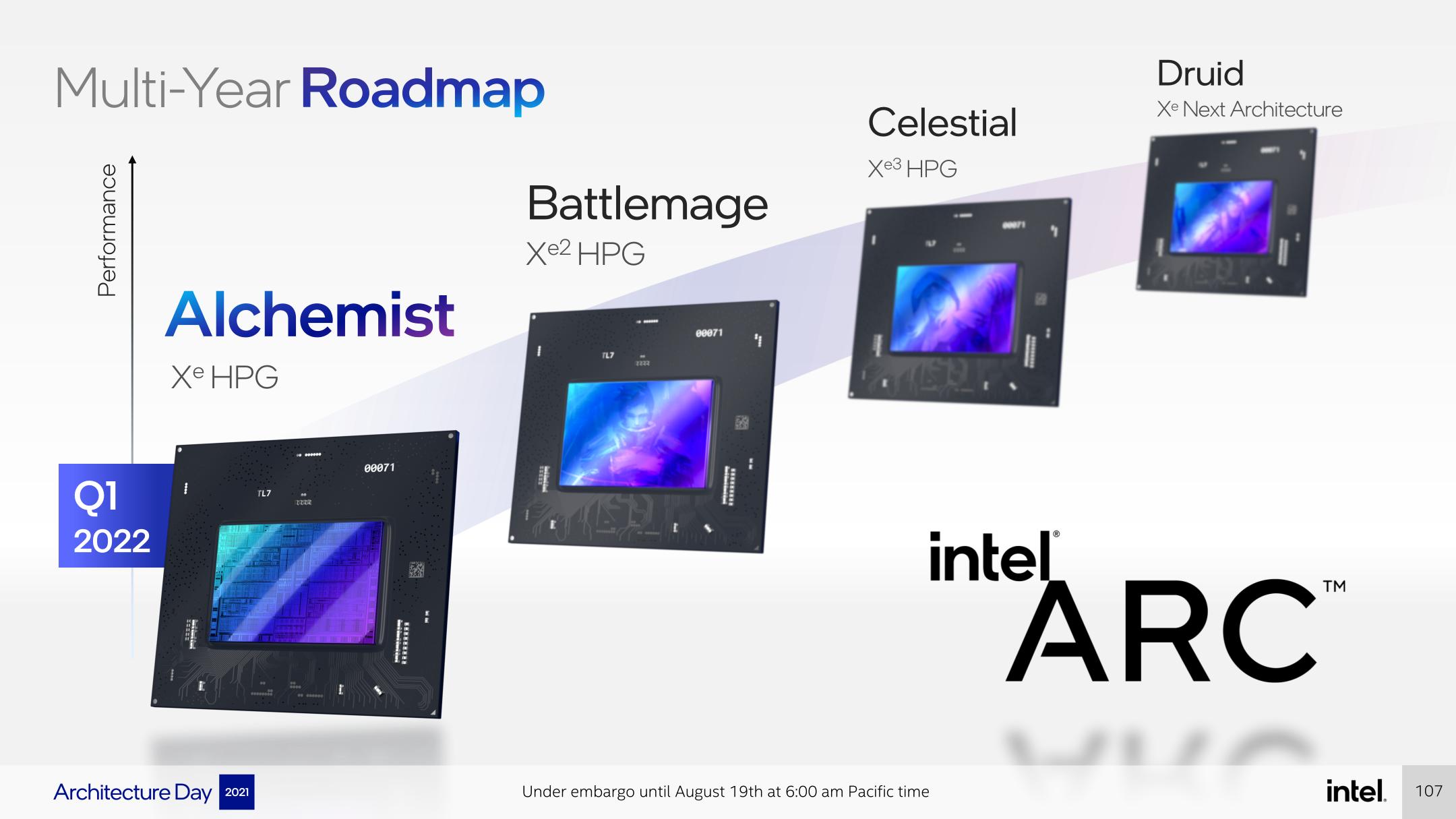
Intel also revealed that they are already hard at work at successive generations, with the Battlemage, Celestial, and Druid architectures all under development for future generations of products. By revealing successive architecture names now, Intel is looking to demonstrate that they are executing on a long-term plan for Xe-HPG that goes several years down the road, and that gamers who jump on board with relative newcomer Intel won’t be quickly abandoned.
Finally, Intel revealed the brand name for their consumer graphics products: Arc. Arc will be Intel’s new brand name for their consumer video cards, as well as the associated software and services. The first Arc products will be launching in Q1 of 2022, with Intel offering Arc products for both mobile discrete graphics as well as the traditional discrete desktop market. As with all Intel quarterly launch windows, we’re working under the assumption that Intel is looking at the later part of the quarter, in which case we’re likely looking at a March launch window.
Intel Architecture Day 2021: A Sneak Peek at Alchemist
Jumping forward to today, as part of their ramp-up to the launch of their first high-performance discrete graphics products, Intel is giving us our first look at the Alchemist Xe-HPG architecture.
The company is eager to show off what they’ve been working on in secret for the last few years. At the same time however, Intel is at least 5 months away from launching these products, and they’re well aware of this fact. Consequently, today’s disclosures from the company are relatively limited, especially compared to what’s being disclosed about Alder Lake CPUs, or even Xe-LP during last year’s architecture day. There are some things like clockspeed and performance where Intel is simply too far out to offer concrete details; and in other areas, Intel is holding back information so that they have something to talk about between now and the launch of the first Arc products.
As a result, today’s architecture-focused disclosure on Xe-HPG can best be thought of as a mid-level look at the architecture. Intel is not giving us a look at the lowest level of nuts and bolts such as pipeline latencies and cache sizes, but they are giving us a look at the logical organization of the architecture, and how the various bits fit together. The net result is our most detailed look yet at Alchemist/Xe-HPG, but with plenty of holes that Intel is leaving behind to fill at a later date.
It All Starts With Xe Core (Alchemist Edition)
Even though Intel treats Xe as a family of GPU architectures, in practice these architectures can be quite different from each other. This is true even for Alchemist, where by their own admittance Intel had to rework some of the architectural fundamentals for their GPU relative to Xe-LP, which was introduced only a year ago. To what degree they differ remains to be seen, but it’s clear right off the bat that Intel isn’t treating Alchemist as a bigger Xe-LP design, and that some significant changes have been required to design a GPU with the necessary scalability.
And that differentiation goes down to the fundamental building blocks of their GPUs and how they are logically organized. After many years of using the Execution Unit (EU) as their fundamental compute/shader unit, Intel is tossing that aside, citing how much EUs have changed over the generations, and consequently how difficult it is to compare them.
Instead, starting with Alchemist (and Ponte Vecchio), Intel is introducing a new fundamental building block: the Xe Core.
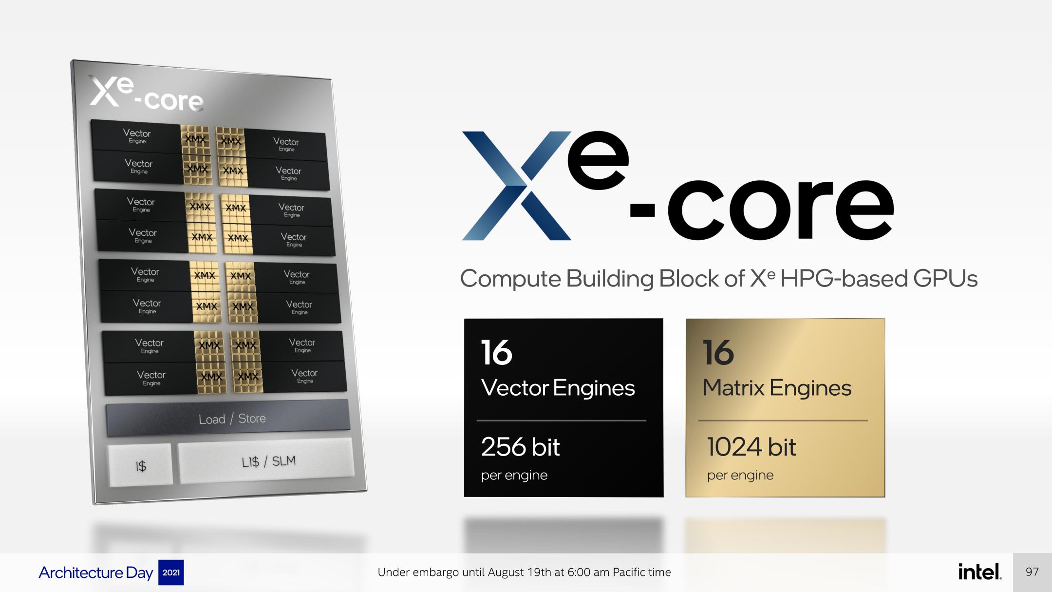
The Xe Core is, at a high level, a collection of vector and matrix (tensor) ALUs, paired with L0/L1 caches load/store units, and no doubt some extended math ALUs as well. At a logical level, this is relatively close in functionality to an Xe-LP subslice or to an NVIDIA SM (minus the texture units), though any internal organizational similarities remain to be seen.
Each Xe Core contains 16 vector units, each which in turn can process 256 bits per cycle. Breaking this down to the most fundamental level, this works out to 8 FP32 ALUs per vector engine, making each vector engine roughly analogous to an Xe-LP EU. And with 16 such vector engines per Xe Core, this means a single Xe Core should be able to process 128 FP32 operations per clock (for 256 FLOPS of FMA throughput). To once again lean on our NVIDIA SM analogy, this is the same throughput per clock as an Ampere SM.
| Intel GPU Compute Throughput Rates (FMA, Ops-per-clock-per-core/subslice) |
||||
| Xe-HPG | Xe-LP | |||
| FP32 | 256 | 256 | ||
| INT8 | DP4A: 1024? Matrix: 4096 |
DP4A: 1024 | ||
Those 16 vector units are also paired with 16 matrix math units for matrix/tensor operations. Exposed via the Xe Matrix eXtensions (XMX) and sometimes labeled as such, these are new to Intel’s GPU architecture, and makes Intel the second discrete GPU manufacturer to start including a systolic array for dense matrix operations. These matrix units can process 1024 bits per clock, which works out to 64 FP16 operations per cycle, or 128 INT8 ops. Multiplied by the 16 matrix units in each Xe Core, and this adds up to 1024 FP16 matrix operations every cycle (2048 FLOPS of FP16 FMA).
More interesting still is that, comparatively speaking, Intel seems to be dedicating an even larger percentage of their hardware to matrix math than NVIDIA. While Intel and NVIDIA are matched in vector throughput at 128 FP32 operations per SM/Xe Core, Intel is offering twice the matrix math throughput – and thus has dedicated twice as many ALUs to the task. All of which means that Intel is seemingly betting big on matrix math and neural network/AI processing being a driving need going forward. Bear in mind that these matrix math units aren’t usable for most basic graphics shader operations (at least in 2021), so Intel is making a serious tradeoff in devoting this much hardware to matrix operations.
Just how Intel intends to fill them remains to be seen. But certainly a part of that equation will be Intel’s Xe Super Sampling (XeSS) technology. The company’s image upscaling technology will rely in part on neural networking models, which in turn will be able to run on the matrix engines.
Rounding out the package is Intel’s collection of load/store units, as well as the L0/L1 caches. Intel tells us that they have beefed up their load/store units to handle the heavy data needs of the matrix engines, however they aren’t going into any further detail at this time. As well, we’re not getting any disclosures on cache sizes today.
Building Up: 4 Cores Makes a Render Slice
Following the basic Xe Core, the next level in Xe-HPG’s logical organization is the render slice, an organizational unit that Intel is keeping from their earlier architectures. And like those earlier architectures, a slice is most of what you need to build a GPU.
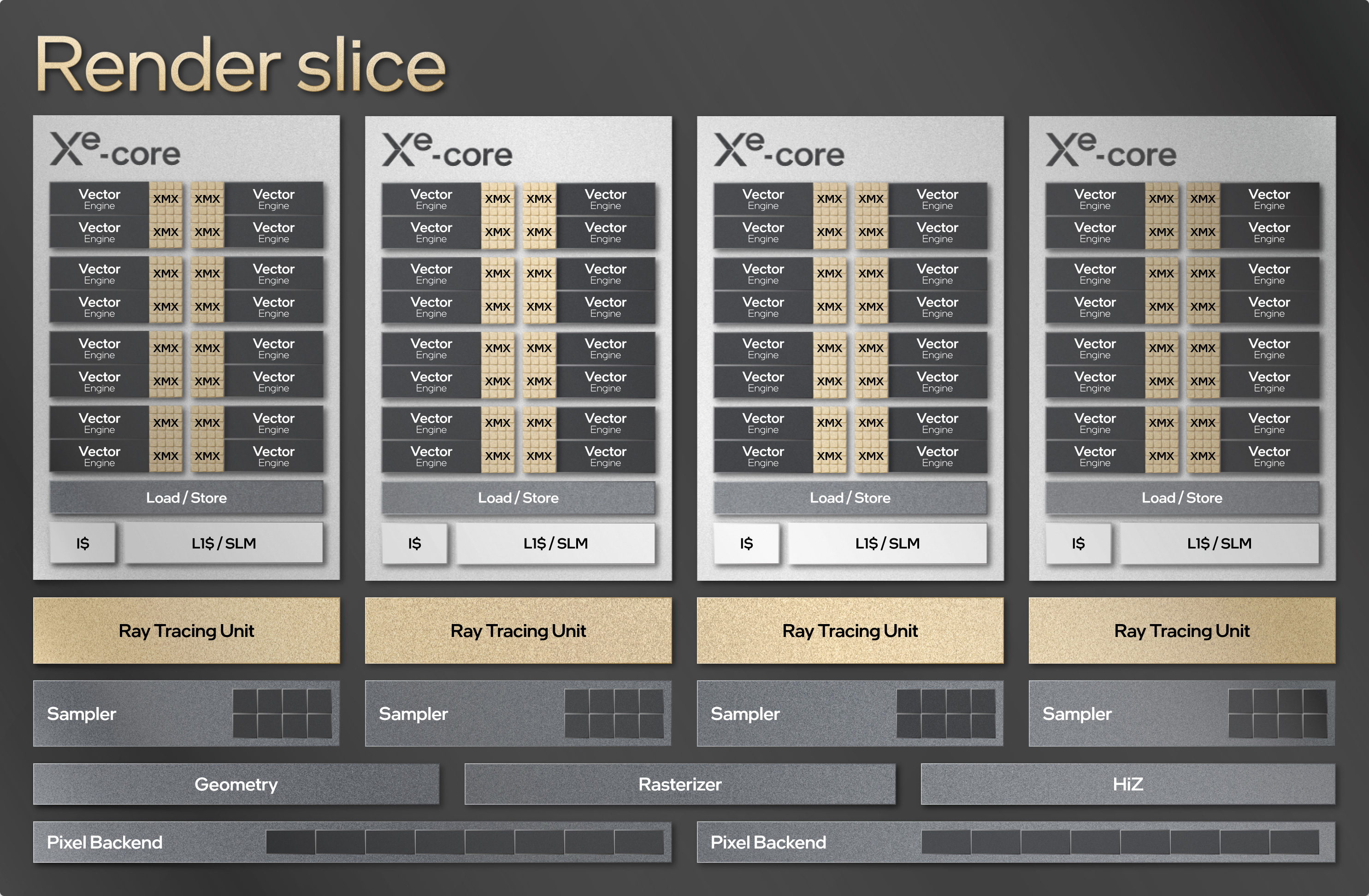
For Alchemist, a slice contains 4 Xe Cores, along with 4 ray tracing units, 4 texture samplers, the geometry/rasterization frontends, and 2 pixel backends (each capable of pushing 8 pixels/clock). Compared to the Xe-LP architecture, this is a leaner setup, with fewer pixel backends and fewer subslices/Xe Cores than the equivalent Xe-LP slice.
In some respects this is a bit more granular than Xe-LP, but at a more fundamental level I suspect the changes are anchored around better balancing the various GPU resources. We don’t have any throughput information on the geo/rasterization hardware, but if it’s anything like Xe-LP, then it means that Intel has scaled up the amount of frontend hardware relative to the rest of their design. Meanwhile, although they’re part of the slice rather than the Xe Core, this 4:4:4 layout means that for Alchemist, each Xe Core essentially has its own texture sampler and ray tracing unit.
Speaking of ray tracing, this is another area where Intel is giving us a bit more detail on the inner-workings of the architecture. Intel is now confirming that their RT units are capable of accelerating ray traversals, bounding box intersections, and triangle intersections. All of which is very similar to what NVIDIA’s own RT cores are capable of. Intel is not talking about the actual performance throughput of these units at this time, so how they will perform remains to be seen.
Making Alchemist Whole: Up to 8 Slices
Last, but not least in our tour of the Alchemist GPU architecture is a look at how a complete GPU is put together. As with previous Intel graphics architectures, Intel will be able to scale up (or down) their designs based on the number of slices. In the case of Alchemist, the architecture can be scaled up to as high as 8 slices, which is two slices larger than Xe-LP.
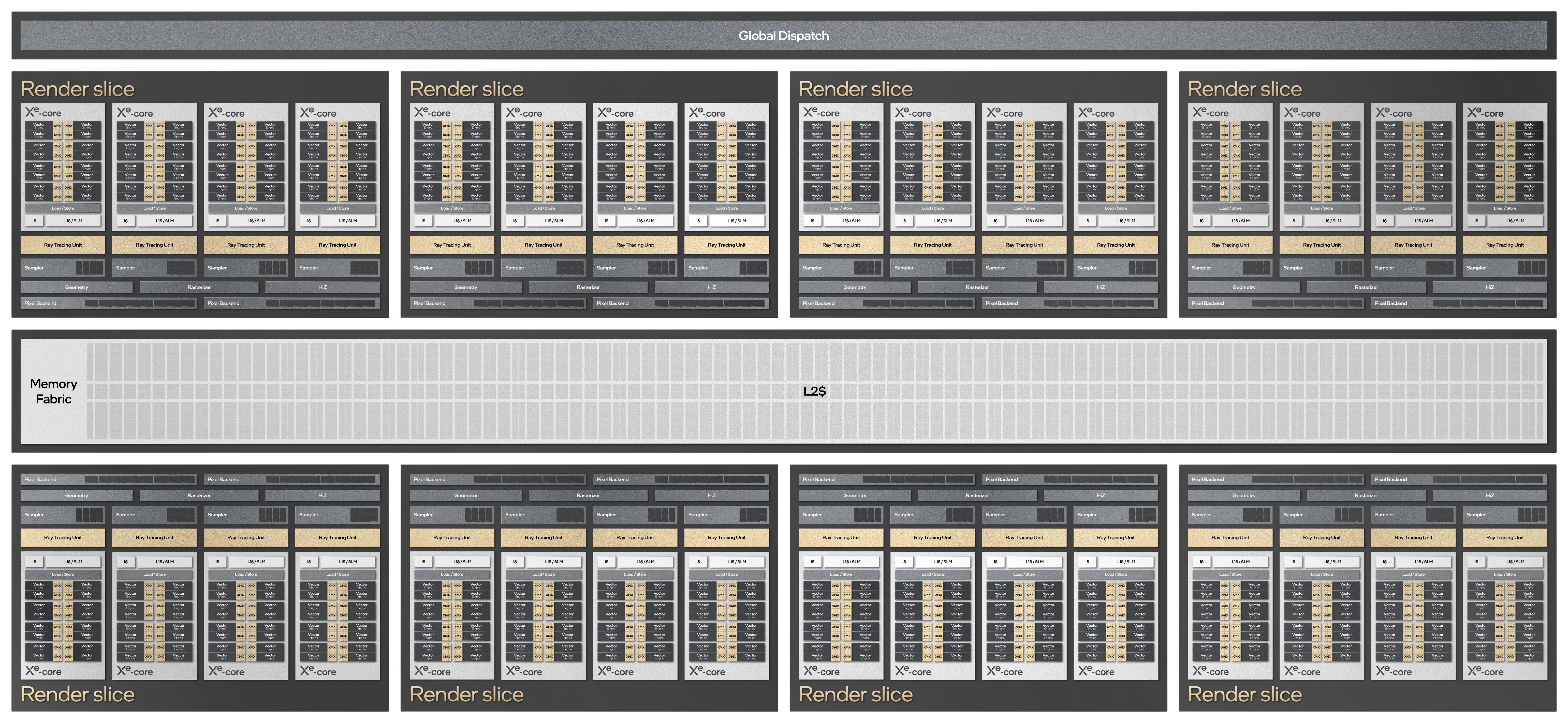
Connecting those slices – and completing the GPU – is the traditional memory fabric backend, which also contains the L2 cache. Meanwhile a global dispatch processor sits at the front end to issue work to the slices and beyond. Intel is not disclosing anything further about these parts today, so we don’t have any information L2 cache sizes, cache bandwidth, or the like.
Not present in Intel’s diagrams but undoubtedly hiding at this level as well are all of the fixed function units such as the PCIe interface, media engine, display controllers, copy engine, and the other pieces that were previously known as the unsliced. Based on some Linux driver commits, there is strong evidence that Intel will support DisplayPort 2.0 with Alchemist, which would make them the first GPU vendor to ship with those capabilities.
Intel also isn’t disclosing anything about retail products or GPU configurations today. So while we know what Alchemist can scale up to, we don’t know what the actual shipping configurations will be. Still, assuming for the moment that Intel aims to ship a full, 8 slice configuration, that means such a chip would offer 32 Xe Cores, or 4096 FP32 ALUs. This is nearly 5x as many vector ALUs as the DG1 Xe-LP GPU, not counting all the additional hardware Intel has added for matrix cores, DirectX 12 Ultimate functionality, and all the other feature additions that come with Alchemist.
Designed By Intel, Built By TSMC: Alchemist Starts At N6
Architecture aside, perhaps the biggest burning question of all has been where Intel would even have its first generation of high-performance Xe-HPG GPUs built at. Though Intel’s lone discrete Xe-LP GPU (DG1) was built on their 10nm process to coincide with Intel’s CPU and integrated GPU needs, Alchemist had no such limitations. In fact it pretty much had to be built outside of Intel, as Intel’s 10nm process is not competitive enough with the likes of TSMC’s 7nm process, which competitor AMD is already using for their GPUs. Which is why Intel revealed as far back as the Xe-HPG announcement that the GPU would be built at an external fab.
As part of today’s architecture day announcements, Intel is finally answering the burning question and disclosing the fab and node being used. As many have expected, Intel is indeed turning to TSMC to fab their gaming GPU, and they will be using TSMC’s N6 process to do it.
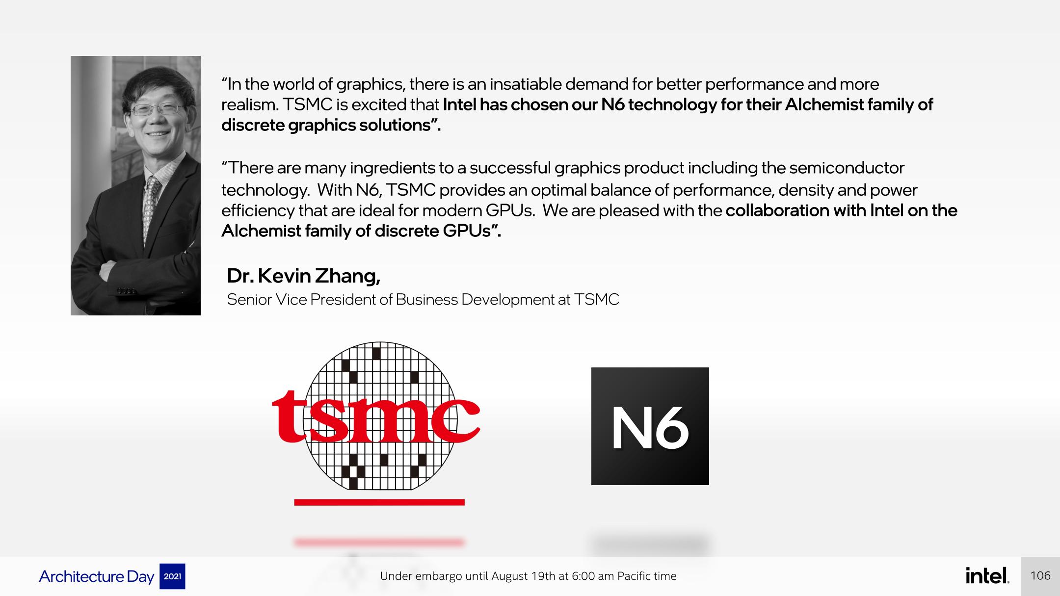
When they ship next year, the Alchemist chips will be the first GPUs built on the N6 process. Though not TSMC’s leading process – that honor belongs to N5 – N6 is the next best choice to ship a GPU on – and likely the only economical one. N6 is essentially an improved version of TSMC’s N7 node, which replaces some DUV layers with EUV layers while retaining most of the same design rules and tools. TSMC hasn’t been promoting the half-node too much on a performance basis – performance is about equal to N7 – but it does take some important steps to simplifying the manufacturing process versus N7. And, especially important for a relatively large die product like a GPU, it offers around 18% improved density versus N7.
Given Intel’s Q1’22 release timeframe, Intel’s Alchemist GPUs will almost certainly be the most advanced consumer GPUs on the market with respect to manufacturing technology. Alchemist will be going up against AMD’s Navi 2x chips built on N7, and NVIDIA’s Ampere GA10x chips built on Samsung 8LPP. That said, as AMD can attest to, there’s more to being competitive in the consumer GPU market than just having a better process node, so Intel’s architecture team still needs to deliver here to make the first generation of Arc produces successful.
Getting Even More: Improving Clockspeeds and Performance-per-Watt for Alchemist
To that end, Intel’s engineers have also been working on Alchemist at a low level to further improve their clockspeeds and performance-per-watt relative to Xe. As we reiterate time and time again, power efficiency is everything for GPUs, as overall GPU performance these days is heavily constrained by TDP. It’s a lot easier to build a bigger/faster GPU than it is to build one that’s still fast while not melting down your system in the process.
This means Intel has been going through the Alchemist design at both the logic and circuit level to squeeze out more power savings, and to remove bottlenecks that would constrain clockspeeds. Unfortunately Intel isn’t offering much more in the way of details as to what they’ve done here, so it’s hard to say if they’ve gone through an intensive top-to-bottom process ala AMD for RDNA, or something a bit more scaled back.
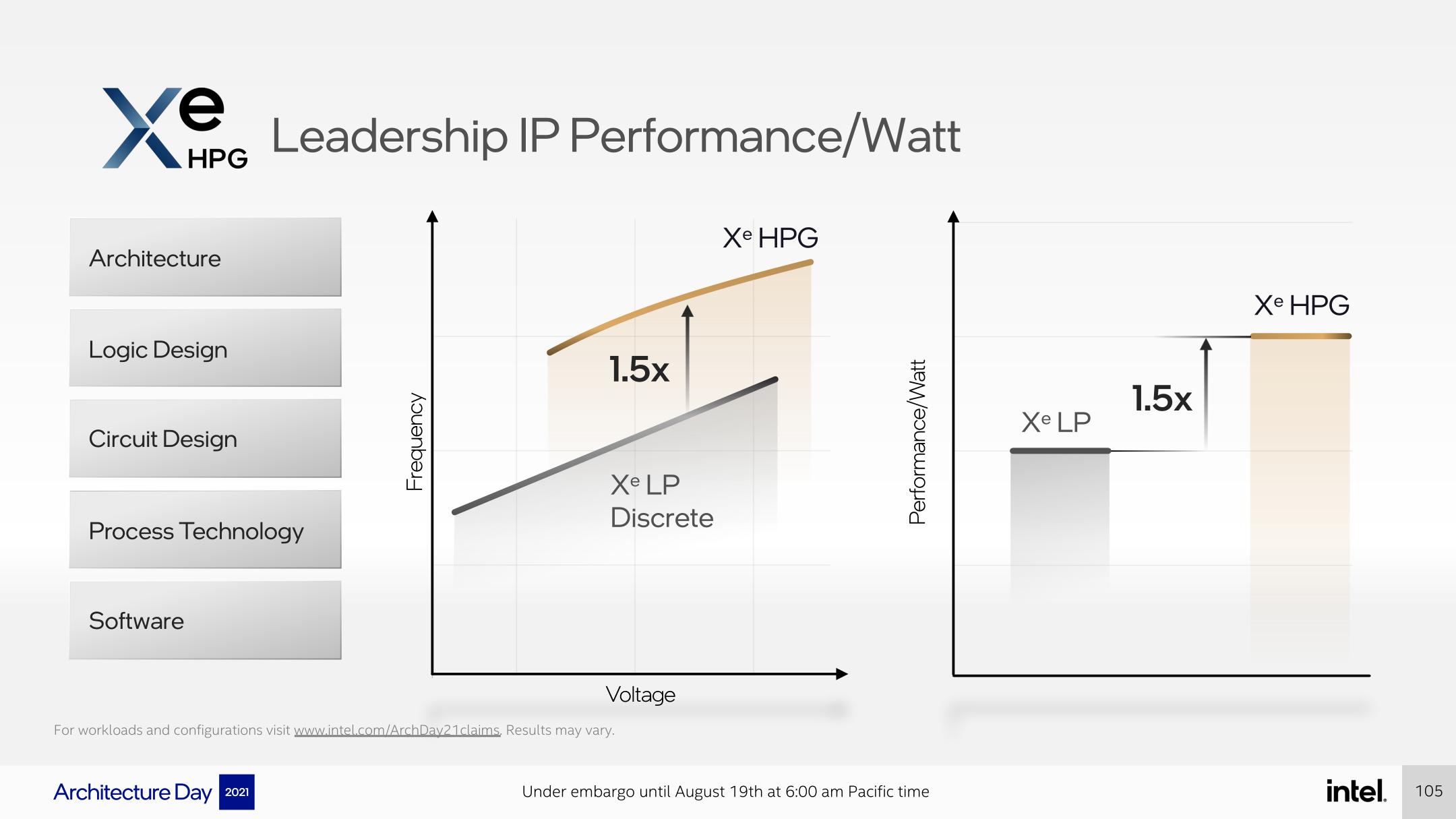
Ultimately, in conjunction with the use of TSMC’s N6 process, Intel is reporting that they’ve improved both their power efficiency (performance-per-watt) and their clockspeeds at a given voltage by 50% compared to Xe-LP. Note that this is the sum total of all of their improvements – process, logic, circuit, and architecture – so it’s not clear how much of this comes from the jump to TSMC N6 from Intel 10SF, and how much comes from other optimizations. But either way, Intel will need everything they can get.
Meanwhile, a 50% clockspeed uplift over Xe-LP would put Intel’s clockspeeds at roughly around 2.4GHz. That would be somewhere in between NVIDIA and AMD, who tend to have slightly lower and higher clockspeeds respectively. Or, to put things in terms of raw throughput, this would give a theoretical 8 slice Alchemist design 18.5 TFLOPS of single precision (FP32) shader/compute throughput, which would be almost 9x the rated throughput of the discrete Xe-LP DG1 video card.
Alchemist & Intel Arc: Coming in Q1 2022
Wrapping things up, for the last four years we’ve been hearing about Intel’s ambitious plans to re-enter the high-performance discrete GPU space. And while it’s going to be a little while longer until their Arc products start shipping, we’re now reached the final countdown. This is the point where Intel ramps up their marketing and their technical disclosures, as they get ready for their Q1 2022 hardware launch.

Today’s Alchemist architecture disclosures in turn are perhaps a bit of a tease, but they are also a hint of what’s to come as Intel launches itself back into the discrete video card market. There are many details we still don’t have right now – everything from memory to GPU configurations and performance expectations – so it would be premature to close this article on anything about performance. That said, I believe it’s safe to say that what will make or break things for Intel in the consumer space is going to be Intel’s own doing. They have access to a leading-edge manufacturing node, countless engineers, and as we’ve just seen, an architecture that, at a high level, seems to offer all the features and functionalities needed to compete and succeed in the discrete graphics market. So we will be watching the next several months with great interest, to see if Intel’s Arc can live up to those ambitions.


72 Comments
View All Comments
mode_13h - Tuesday, October 5, 2021 - link
> I have stated, quite a few times, my reasons for making the effort to talk> about the self-defeating mythology that surrounds PC gaming
Why not indulge us, one more time?
> You continue to try to turn everything into a referendum on my character.
You make it almost impossible not to, with your continual whining, off-topic thread-jacks, leftist propaganda, and anti-AMD conspiracy theories.
> Your debating skills are childish.
If yours were any good, maybe you'd win a few people over to your side. Calling everything a fallacy, as if such allegations are self-evident, self-supporting, and themselves infallible pretty soon just comes off more as laziness than even elitist tone to which you seem to aspire.
shabby - Thursday, August 19, 2021 - link
Watch intel give these away with every desktop at a discounted rate.Drumsticks - Thursday, August 19, 2021 - link
Arc on N6 is interesting for a couple of reasons. First, what the article notes, the extra density advantage that Intel will have. But on top of that, presumably, it means that the capacity dedicated to currently manufacturing AMD and Nvidia N7 GPUs won't be just competing with an additional manufacturer, because Intel is on a separate fab line, presumably we will actually get an increase in the total # of GPUs being put out per month, rather than just seeing the same capacity spread across three companies. If that's true, I wonder if the amount of GPUs AMD or Nvidia can produce on N6 relative to N7 might be a factor in them staying on N7 longer.Granted, of course, I'm sure all of this has been worked out by all four companies well in advance, but it's exciting times. Here's to a third successful manufacturer, and more competition! Now all we need is for Nvidia to somehow jump into the CPU game as a viable Desktop CPU maker, and we'll have a double triple market (not that this one is actually likely!)
Ryan Smith - Thursday, August 19, 2021 - link
"presumably, it means that the capacity dedicated to currently manufacturing AMD and Nvidia N7 GPUs won't be just competing with an additional manufacturer, because Intel is on a separate fab line"N6 makes significant use of TSMC's N7 infrastructure. So they should be considered shared lines for most matters.
dotjaz - Thursday, August 19, 2021 - link
N6 uses the same design rules not the same litho machines. You can't just inject and remove EUV machines from the same production process. N6 would have its own set of EUV and DUV scanners (initially) likely upgraded from the discontinued N7+ line.Drumsticks - Thursday, August 19, 2021 - link
Ah, drat. I guess on the possible bright side, is TSMC still bringing/converting additional capacity to 7(6)nm?mode_13h - Friday, August 20, 2021 - link
> Nvidia to somehow jump into the CPU game as a viable Desktop CPU makerIt's not quite the same thing, but Nvidia is working with MediaTek on gaming-capable ARM SoCs for laptops and potentially even SFF desktop machines.
https://nvidianews.nvidia.com/news/nvidia-and-part...
(search for mediatek)
BedfordTim - Thursday, August 19, 2021 - link
Everything I read suggests there is substantial brand loyalty/hatred in the GPU market, but maybe that is a vocal few.euskalzabe - Thursday, August 19, 2021 - link
Many people (stupidly) love to pick sides. With intel in the game/war, it'll become one more side to pick. Who cares, if we get more GPUs, and with intel needing to establish itself as a serious player, if we get better price/performance ratios, this is nothing but welcome news in our very stagnant GPU industry.mode_13h - Friday, August 20, 2021 - link
What gets people really animated is when they sense unfair dealing. Like if one GPU maker develops proprietary libraries tuned for their hardware, and incentives some game developers to use them.Another big thing source of conflict is when companies misrepresent their products, such as via benchmark-rigging.
> very stagnant GPU industry.
It's certainly not stagnant in terms of feature set or performance!