Intel’s Integrated Graphics Mini-Review: Is Rocket Lake Core 11th Gen Competitive?
by Dr. Ian Cutress on May 7, 2021 10:20 AM EST
In the last few months we have tested the latest x86 integrated graphics options on the desktop from AMD, with some surprising results about how performant a platform with integrated graphics can be. In this review, we’re doing a similar test but with Intel’s latest Rocket Lake Core 11th Gen processors. These processors feature Intel’s Xe-LP graphics, which were touted as ‘next-generation’ when they launched with Intel’s mobile-focused Tiger Lake platform. However, the version implemented on Rocket Lake has fewer graphics units, slower memory, but a nice healthy power budget to maximize. Lo, Intel set forth for battle.
When a CPU meets GPU
Intel initially started integrating graphics onto its systems in 1999, by pairing the chipset with some form of video output. In 2010, the company moved from chipset graphics to on-board processor graphics, enabling the graphics hardware to take advantage of a much faster bandwidth to main memory as well as a much lower latency. Intel’s consumer processors now feature integrated graphics as the default configuration, with Intel at times dedicating more of the processor design to graphics than to actual cores.
| Intel CPUs: IGP as a % of Die Area | ||||||
| AnandTech | Example | Launched | Cores | IGP | Size | IGP as Die Area % |
| Sandy Bridge | i7-2600K | Jan 2011 | 4 | Gen6 | GT2 | 11% |
| Ivy Bridge | i7-3770K | April 2012 | 4 | Gen7 | GT2 | 29% |
| Haswell | i7-4770K | June 2013 | 4 | Gen7.5 | GT2 | 29% |
| Broadwell | i7-5775C | June 2015 | 4 | Gen8 | GT3e | 48% |
| Skylake | i7-6700K | Aug 2015 | 4 | Gen9 | GT2 | 36% |
| Kaby Lake | i7-7700K | Jan 2017 | 4 | Gen9 | GT2 | 36% |
| Coffee Lake | i7-8700K | Sept 2017 | 6 | Gen9 | GT2 | 30% |
| Coffee Lake | i9-9900K | Oct 2018 | 8 | Gen9 | GT2 | 26% |
| Comet Lake | i9-10900K | April 2020 | 10 | Gen9 | 24 EUs | 22% |
| Rocket Lake | i9-11900K | March 2021 | 8 | Xe-LP | 32 EUs | 21% |
| Mobile CPUs | ||||||
| Ice Lake-U | i7-1065G7 | Aug 2019 | 4 | Gen11 | 64 EUs | 36% |
| Tiger Lake-U | i7-1185G7 | Sept 2020 | 4 | Xe-LP | 96 EUs | 32% |
All the way from Intel’s first integrated graphics to its 2020 product line, Intel was reliant on its ‘Gen’ design. We saw a number of iterations over the years, with updates to the function and processing ratios, with Gen11 featuring heavily in Intel’s first production 10nm processor, Ice Lake.
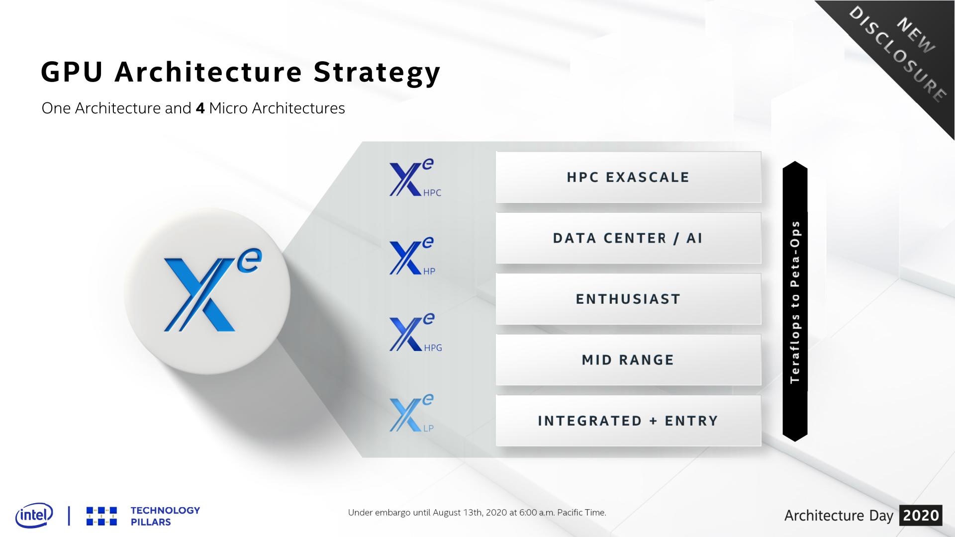
The latest graphics design however is different. No longer called ‘Gen’, Intel upcycled its design with additional compute, more features, and an extended effort for the design to scale from mobile compute all the way up to supercomputers. This new graphics family, known as Xe, is now the foundation of Intel’s graphics portfolio. It comes in four main flavors:
- Xe-HPC for High Performance Computing in Supercomputers
- Xe-HP for High Performance and Optimized FP64
- Xe-HPG for High Performance Gaming with Ray Tracing
- Xe-LP for Low Power for Integrated and Entry Level
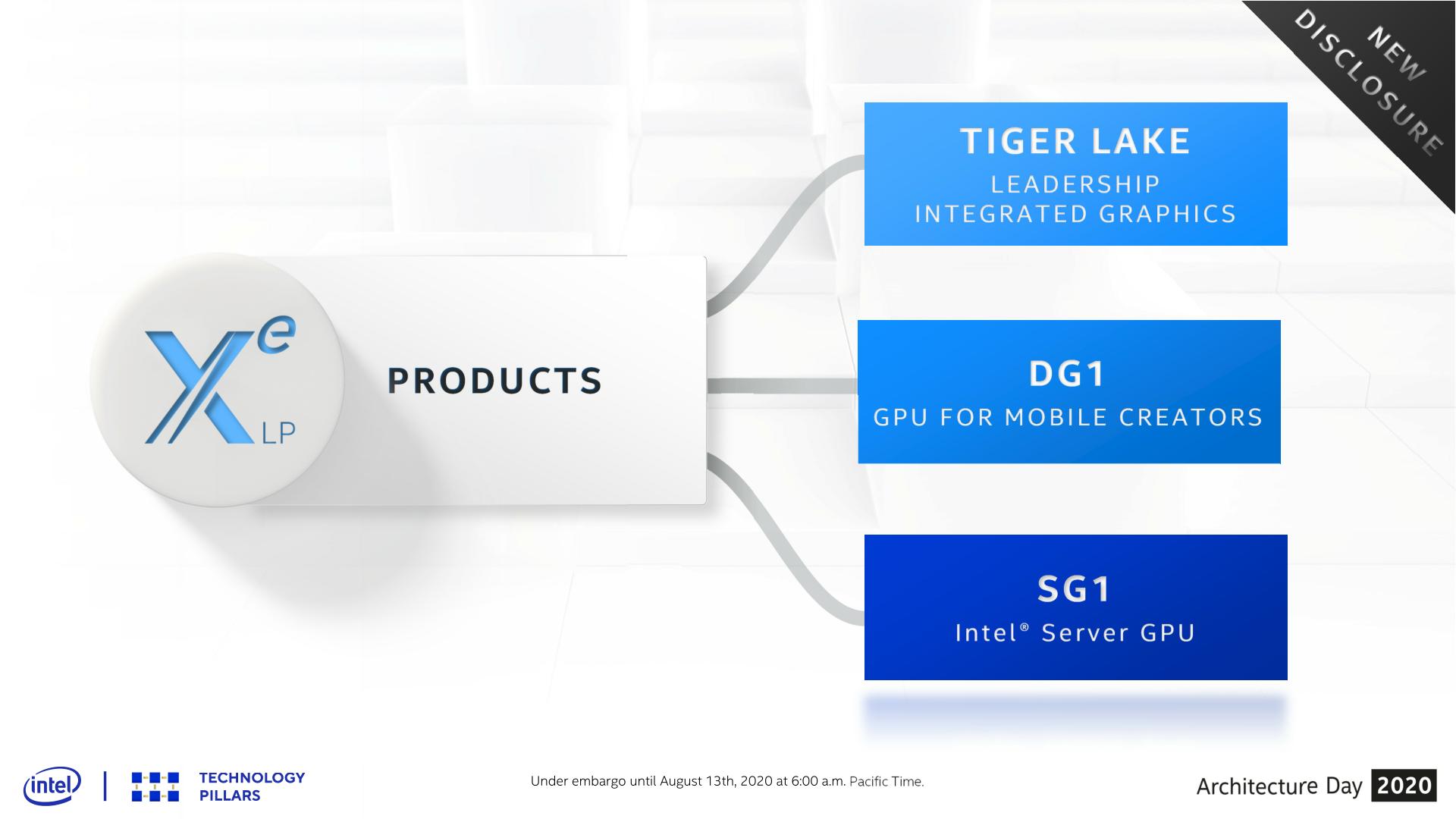
Intel has initially rolled out its LP designs into the market place, first with its Tiger Lake mobile processors, then with its Xe MAX entry level notebook graphics card, and now with Rocket Lake.
Xe-LP, A Quick Refresher
Intel’s LP improves on the previous Gen11 graphics by reorganizing the base structure of the design. Rather than 7 logic units per execution unit, we now have 8, and LP’s front-end can dispatch up two triangles per clock rather than one. The default design of LP involves 96 execution units, split into a centralized ‘slice’ that has all the geometry features and fixed function hardware, and up to 6 ‘sub-slices’ each with 16 logic units and 64 KiB of L1 cache. Each variant of LP can then have up to 96 execution units in a 6x16 configuration.
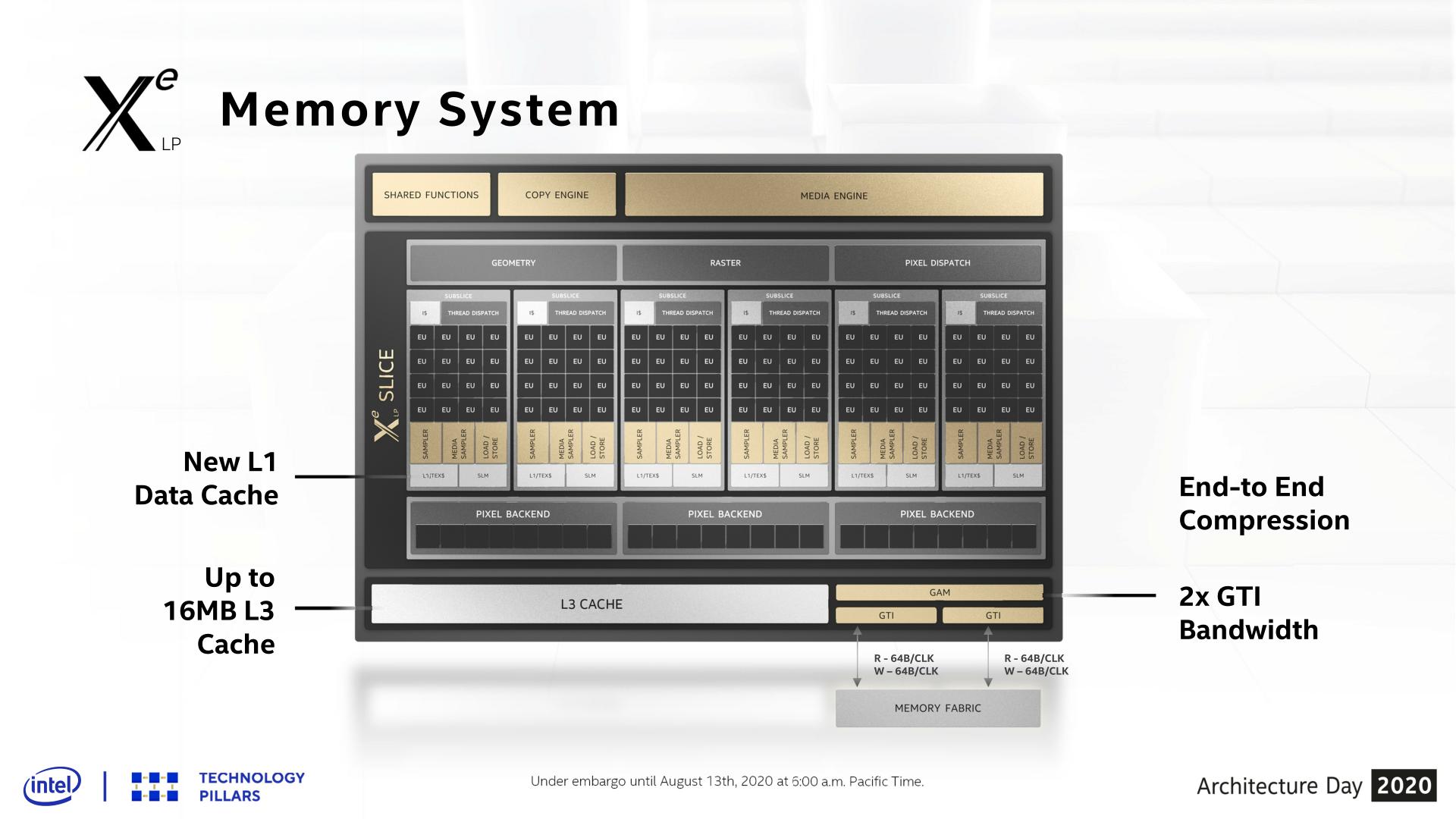
Execution units now work in pairs, rather than on their own, with a thread scheduler shared between each pair. Even with this change, each individual execution unit has moved to an 8+2 wide design, with the first 8 working on FP/INT and the final two on complex math. Previously we saw something more akin to a 4+4 design, so Intel has rebalanced the math engine while also making in larger per unit. This new 8+2 design actually decreases the potential of some arithmetic directly blocking the FP pipes, improving throughput particularly in graphics and compute workloads.
The full Tiger Lake LP solution has all 96 execution units, with six sub-slices each of 16 execution units (6x16), Rocket Lake is neutered by comparison. Rocket Lake has 4 sub-slices, which would suggest a 64 execution unit design, but actually half of those EUs are disabled per sub-slice, and the final result is a 32 EU implementation (4x8). The two lowest Rocket Lake processors have only a 3x8 design. By having only half of each sub-slide active, this should in theory give more cache per thread during operation, and provides less cache pressure. Intel has enabled this flexibility presumably to provide a lift in edge-case graphics workloads for the parts that have fractional sub-slices enabled.
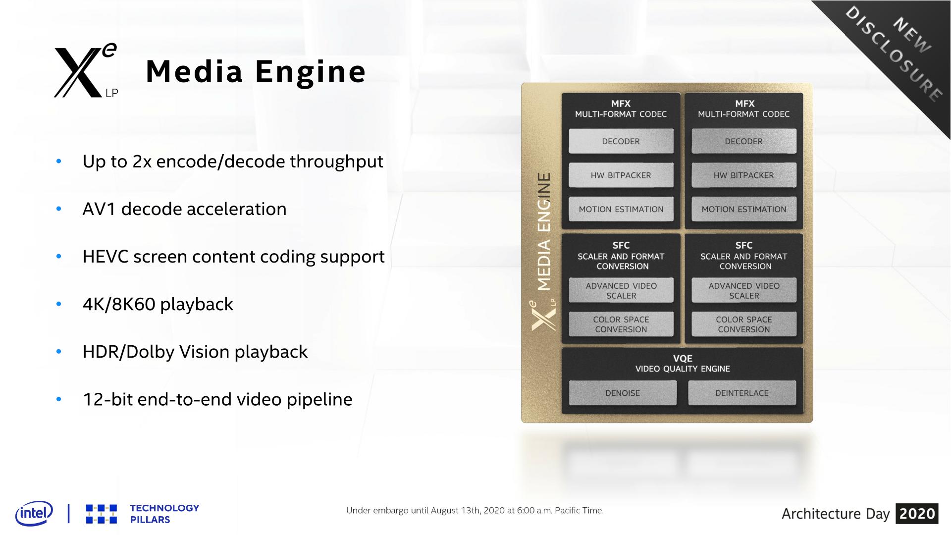
Xe-LP also comes with a revamped media engine. Along with a 12-bit end-to-end video pipeline enabling HDR, there is also HEVC coding support and AV1 decode, the latter of which is a royalty-free codec providing reported similar or better quality than HEVC. Intel is the first desktop IGP solution to provide AV1 accelerated decode support.
Rocket Lake Comparisons
For this review, we are using the Core i9-11900K, Core i7-11700K, and Core i5-11600K. These three are the highest power processors in Intel’s Rocket Lake lineup, and as a result they support the highest configuration of LP graphics that Intel provides on Rocket Lake. All three processors have a 4x8 configuration, and a turbo frequency up to 1300 MHz.
| Intel Integrated Graphics | |||||
| AnandTech | Core i9 11900K |
Core i7 11700K |
Core i5 11600K |
Core i9 10900K |
|
| Cores | 8 / 16 | 8 / 16 | 6 / 12 | 10 / 20 | |
| Base Freq | 3500 MHz | 3600 MHz | 3900 MHz | 3700 MHz | |
| 1T Turbo | 5300 MHz | 5000 MHz | 4900 MHz | 5300 MHz | |
| GPU uArch | Xe-LP | Xe-LP | Xe-LP | Gen 11 | |
| GPU EUs | 32 EUs | 32 EUs | 32 EUs | 24 EUs | |
| GPU Base | 350 MHz | 350 MHz | 350 MHz | 350 MHz | |
| GPU Turbo | 1300 MHz | 1300 MHz | 1300 MHz | 1200 MHz | |
| Memory | DDR4-3200 | DDR4-3200 | DDR4-3200 | DDR4-2933 | |
| Cost (1ku) | $539 | $399 | $262 | $488 | |
Our comparison points are going to be Intel’s previous generation Gen11 graphics, as tested on the Core i9-10900K which has a 24 Execution Unit design, AMD’s latest desktop processors, a number of Intel’s mobile processors, and a discrete graphics option with the GT1030.
In all situations, we will be testing with JEDEC memory. Graphics loves memory bandwidth, and CPU memory controllers are slow by comparison to mobile processors or discrete cards; while a GPU might love 300 GB/s from some GDDR memory, a CPU with two channels of DDR4-3200 will only have 51.2 GB/s. Also, that memory bank needs to be shared between CPU and GPU, making it all the more complex. The use case for most of these processors on integrated graphics will often be in prebuilt systems designed to a price. That being said, if the price of Ethereum keeps increasing, integrated graphics might be the only thing we have left.
The goal for our testing comes in two flavors: Best Case and Best Experience. This means for most benchmarks we will be testing at 720p Low and 1080p Max, as this is the area in which integrated graphics is used. If a design can’t perform at 720p Low, then it won’t be going anywhere soon, however if we can achieve good results at 1080p Max in certain games, then integrated graphics lends itself as a competitive option against the basic discrete graphics solutions.
If you would like to see the full CPU review of these Rocket Lake processors, please read our review:
Intel Rocket Lake (14nm) Review: Core i9-11900K, Core i7-11700K, and Core i5-11600K
Pages In This Review
- Analysis and Competition
- Integrated Graphics Gaming
- Conclusions and Final Words


165 Comments
View All Comments
mode_13h - Friday, May 7, 2021 - link
> I didn't see that the title question was answered in the articleI think they presume that piece of meat behind your eyes is doing more than keeping your head from floating away. Look at the graphs, and see the answer for yourself.
However, the article does in fact sort of answer it, in the title of the final page:
"Conclusions: The Bare Minimum"
mode_13h - Friday, May 7, 2021 - link
> unless Dr. Ian Cutress is asking whether Intel's current IGPs are "competitive"> with older Intel IGPs...which would seem to be the case.
As is often the case, they're comparing it with previous generations that readers might be familiar with, in order to get a sense of whether/how much better it is.
And it's not as if that's *all* they compared it against!
dwillmore - Friday, May 7, 2021 - link
So your choices are postage stamp or slide show? No thank you.Oxford Guy - Friday, May 7, 2021 - link
My favorite part of the Intel CPU + Intel GPU history is Atom, where serious hype was created over how fabulously efficient the chip was, while it was sold with a GPU+chipset that used — what was it? — three times the power — negating the ostensible benefit from paying for the pain of an in-order CPU (a time-inefficient design sensibly abandoned after the Pentium 1). The amazing ideological purity of the engineering team’s design goal (maximizing the power efficiency of the CPU) was touted heavily. Netbooks were touted heavily. I said they’re a mistake, even before I learned (which wasn’t so easy) that the chipset+GPU solution Intel chose to pair with Atom (purely to save the company money) made the whole thing seem like a massive bait and switch.mode_13h - Friday, May 7, 2021 - link
> fabulously efficient the chip was, while it was sold with a GPU+chipset that used> — what was it? — three times the power
Well, if they want to preserve battery life, maybe users could simply avoid running graphically-intensive apps on it? I think that's a better approach than constraining its graphics even further, which would just extend the pain.
I'm also confused which Atoms you mean. I'm not sure, but I think they didn't have iGPUs until Silvermont, which was already an out-of-order core. And those SoC's only had 4 EUs, which I doubt consumed 3x the power of the CPU cores & certainly not 3x the power of the rest of the chip.
What I liked best about Intel's use of their iGPUs in their low-power SoCs is that the drivers just work. Even in Linux, these chips were well-supported, pretty much right out of the gate.
TheinsanegamerN - Friday, May 7, 2021 - link
Graphically intensive apps, you mean like windows explorer and a web browser? Because that was enought o obliterate battery life.The original atom platform was awful. Plain and simple.
29a - Friday, May 7, 2021 - link
This^ Atoms were awful turning the computer on would be considered graphically intensive.mode_13h - Friday, May 7, 2021 - link
I still don't follow the logic of the Oxford dude. Would it really have been a good solution to put in even worse graphics, further impinging on the user experience, just to eke out a little more battery life? I'm not defending the overall result, but that strikes me as an odd angle on the issue.Indeed, if explorer and web browser were as much as their GPU could handle, then it seems the GPU was well-matched to the task.
Oxford Guy - Sunday, May 9, 2021 - link
You should learn about the Atom nonsense before posting opinions about it.The power consumption chipset + GPU completely negated the entire point of the Atom CPU, from its design philosophy to the huge hype placed behind it by Intel, tech media, and companies peddling netbooks.
It is illustrative of large-scale bait and switch in the tech world. It happened purely because Intel wanted to save a few pennies, not because of technological restriction. The chipset + GPU could have been much more power-efficient.
Spunjji - Monday, May 10, 2021 - link
You don't follow because you're trying to assess what he said by your own (apparently incomplete) knowledge, whereas what would make sense here would be to pay more attention to what he said - because, in this case, it's entirely accurate.Intel paired the first 45nm Atom chips with one of two chipsets - either the recycled 180nm 945 chipset, designed for Pentium 4 and Core 2 processors, or the 130nm Poulsbo chipset. The latter had an Imagination Technologies mobile-class GPU attached, but Intel never got around to sorting out working Windows drivers for it. In either case, it meant that they'd built an extremely efficient CPU on a cutting-edge manufacturing process and then paired it with a hot, thirsty chipset. It was not a good look; this was back when they were absolutely clobbering TSMC on manufacturing, too, so it was a supreme own-goal.