The Ampere Altra Review: 2x 80 Cores Arm Server Performance Monster
by Andrei Frumusanu on December 18, 2020 6:00 AM EST- Posted in
- Servers
- Neoverse N1
- Ampere
- Altra
1st Generation Neoverse-N1 80-Core Server SoC
For readers who are familiar with the Neoverse-N1 and our coverage of the Amazon Graviton2, won’t be too surprised at the general system architecture of the new first generation Altra “Quicksilver” design.
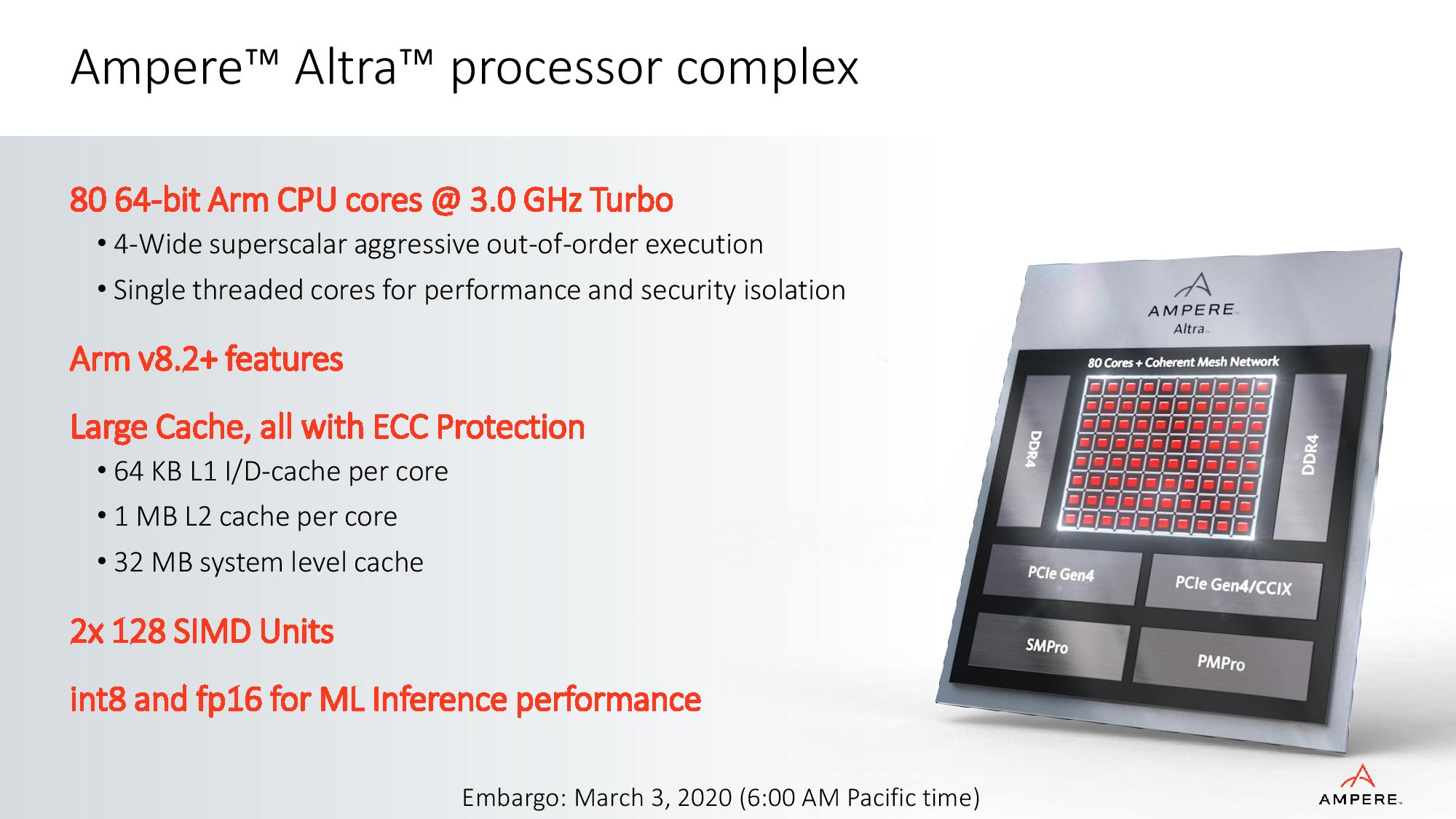
The Quicksilver design features up to 80 Neoverse-N1 cores, integrated within an Arm CMN-600 mesh interconnect that features 32MB of distributed system level cache.
Ampere has equipped the CPU cores themselves with the maximum 64KB L1 caches as well as 1MB of private L2 per core. Although the L3 (the SLC) seems quite reasonable at 32MB, this is actually the same size as the 64-core Graviton2 design, meaning the new Altra system actually gets less cache per core at a system level, which is a bit concerning as we also saw the Graviton2 be quite cache-starved in some workloads. Arm had envisioned Neoverse-N1 systems with either 64MB or even 128MB of L3 cache – it’s a practical compromise in this first-generation product, and we’ll investigate the performance impact later throughout the review.
Beyond the higher core-count, what also stands out for the Altra system in comparison to the Graviton2 are the significantly higher clock frequencies up to 3.3GHz for the top SKU, compared to the 2.5GHz of the Amazon chip – a 32% difference that should lead in a corresponding per-core performance advantage for the Ampere system.
On a system side, the Altra Quicksilver chip features 8 DDR4-3200 memory controllers for a theoretical peak 204GB/s per socket bandwidth.
Ampere achieves dual-socket connectivity through two dedicated PCIe Gen4 x16 links at 25GT/s featuring CCIX protocol compatibility. The bandwidth here is half of a comparable AMD Rome system which features up to 4x x16 Gen4 links between sockets, and it’s also the first time we’ll be seeing CCIX’s cache coherency capabilities used in this way, so that’s definitely a unique design on the part of the Altra system.
Altra QuickSilver SKU List
Ampere had revealed their QuickSilver SKU list earlier this summer, but hadn’t yet published prices for the different configuration, something we can finally reveal today:
| Ampere 1st Gen Altra 'QuickSilver' Product List |
||||||
| AnandTech | Cores | Frequency | TDP | PCIe | DDR4 | Price |
| Q80-33 (Tested) |
80 | 3.3 GHz | 250 W | 128x G4 | 8 x 3200 | $4050 |
| Q80-30 | 80 | 3.0 GHz | 210 W | 128x G4 | 8 x 3200 | $3950 |
| Q80-26 | 80 | 2.6 GHz | 175 W | 128x G4 | 8 x 3200 | $3810 |
| Q80-23 | 80 | 2.3 GHz | 150 W | 128x G4 | 8 x 3200 | $3700 |
| Q72-30 | 72 | 3.0 GHz | 195 W | 128x G4 | 8 x 3200 | $3590 |
| Q64-33 | 64 | 3.3 GHz | 220 W | 128x G4 | 8 x 3200 | $3810 |
| Q64-30 | 64 | 3.0 GHz | 180 W | 128x G4 | 8 x 3200 | $3480 |
| Q64-26 | 64 | 2.6 GHz | 125 W | 128x G4 | 8 x 3200 | $3260 |
| Q64-24 | 64 | 2.4 GHz | 95 W | 128x G4 | 8 x 3200 | $3090 |
| Q48-22 | 48 | 2.2 GHz | 85 W | 128x G4 | 8 x 3200 | $2200 |
| Q32-17 | 32 | 1.7 GHz | 45 W | 128x G4 | 8 x 3200 | $800 |
Ampere here covers a very wide spectrum of SKUs, ranging from today’s tested top-model in the form of the 80-core, 3.3GHz 250W Q80-33, down to “small” low-power 32-core 1.7GHz 45W models such as the Q32-17.
Ampere should be praised for their naming scheme here as it’s the most straightforward of any vendor in the industry, directly showcasing the core number and frequency in the model name, with TDP being really the only characteristic which you’d have to look up.
Across the board, all SKUs feature full 128x lanes of PCIe I/O connectivity, and the full 8-channel DDR4-3200 memory capabilities, capable of hosting up to 4TB of DRAM on all models without any artificial feature limitations.
With today’s reveal of the SKU pricing, we finally can make rough comparisons to Intel’s and AMD’s line-up, and Ampere here is incredibly aggressive in terms of their value proposition as they’re vastly undercutting the competition’s models.
An AMD EPYC 7742 with 64 cores and 225W TDP comes in at $6950, while an Intel Xeon Platinum 8280 with 28 cores and 205W TDP comes in at a price tag of $10009 (It's to be noted that a Xeon Gold 6258R features the same specifications as the 8280 - minus the ability to scale beyond 2 sockets, for only $3950). Ampere’s Q80-33 with 80 cores at a 250W TDP comes a price tag of “only” $4050 seems a steal.
Of course, we’re comparing MSRP to MSRP across vendors – and it’s pretty certain large customers making large order won’t be paying MSRP prices – however if this relative MSRP price positioning between vendors is indicative of pricing for larger orders then Ampere is certain to make a large impact on the enterprise market.
I’m writing this as I know the performance of the new Altra system which we’ll expose in the coming pages – so we’ll revisit whole value proposition argument later on in the article.
About TDPs and Frequencies
One important topic I wanted touch upon was the way Ampere describes TDP and frequencies, as it differs considerably from what the public has gotten used to based on AMD or Intel products.
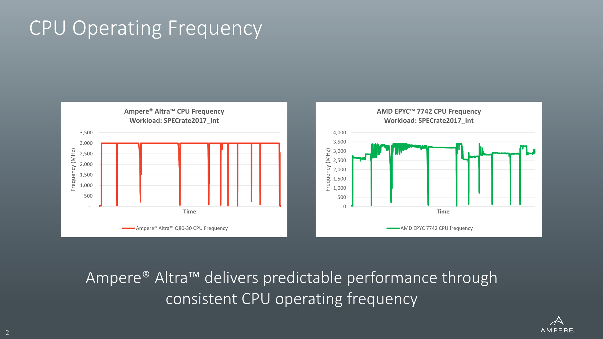
In regards to the described top frequency of the Altra systems, although Ampere calls this a “sustained turbo”, using the turbo nomenclature at all is probably the wrong way to go about it. The peak frequency of the design is simply that – a peak frequency at which the chip normally operates in 99% of scenarios.
This is in contrast to current x86 designs which have “opportunistic turbo” mechanisms which boost their frequencies beyond a guaranteed “base frequency”. In Ampere’s case, the Altra’s described frequency is essentially the de-facto base frequency even though it still operates a normal DVFS scheme and can clock down below that figure during idle or lower utilisation periods.
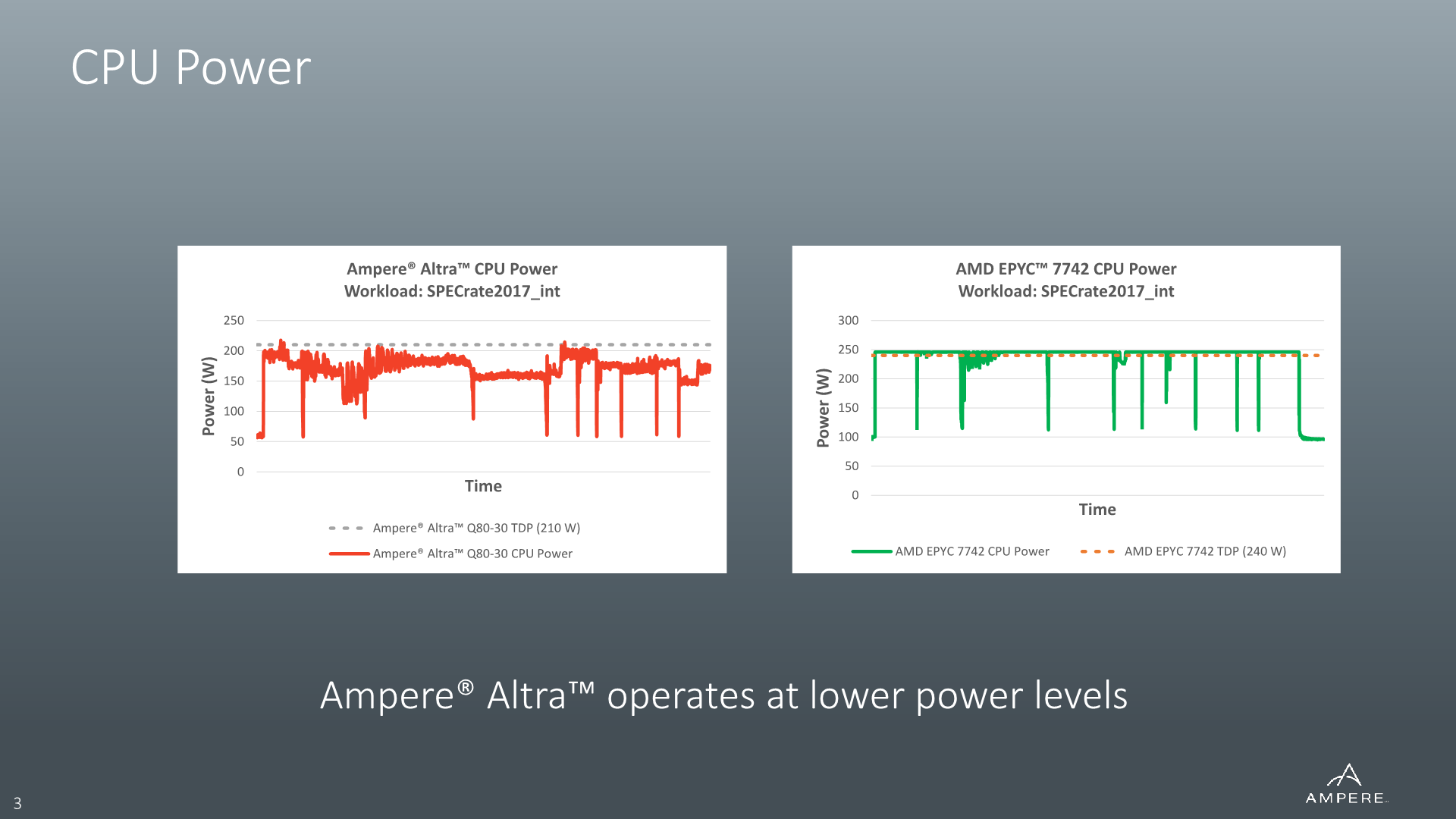
Because frequency is essentially fixed under most workloads, what actually fluctuates between different types of workloads is the power consumption of the processor. The figure described as TDP by Ampere here is the maximum peak small-period average power consumption by the processor.
This comes in contrast to the TDP figures of other systems such as AMD’s EPYC and Xeon CPUs, where the TDP can actually interpreted as a pretty accurate average power consumption figure for the vast majority of workloads. If the processor here under load of a workload that doesn’t particularly result in high power consumption, the designs here will simply increase performance and power by increasing the clock frequency of the design.
For example, a low-IPC high-memory workload on an EPYC 7742 will result in low power consumption on the part of the cores, so the chip will clock them up to 3200MHz on all 64 cores to fill the 225W TDP. A high-IPC workload that stresses the cores and result in higher power might end up with an average runtime frequency of 2600MHz across all cores – but in both cases the average power consumption will always settle around the 225W TDP figure.

So, although for example Ampere’s Altra Q80-33 showcases a 250W TDP figure, its power consumption for the majority of workloads almost always averages below that figure, ranging as low as 180W for some low-IPC workloads. I haven’t actually measured a single average figure across all of our workloads, but a rough estimate across the board for the Q80-33 would be 200W.
In our testing with the Mount Jade server which still had preliminary firmware and which initially had an uncapped TDP, I’ve only ever hit one workload (507.cactuBSSN_r) that consistently broke power consumption in excess of 250W, reaching up to 280W. Re-enabling the TDP cap to 250W of course limited it to that figure on small timescale averages – the Altra’s power management works on a 200µs granularity.
Fundamentally, the Altra’s handling of frequency and power in such a manner is simply a by-product of the Neoverse-N1 cores not being able to clock in higher than 3.3GHz, and the cores being so efficient, that they have power leeway in many workloads, while the x86 player’s implementations simply clock in higher when given the opportunity, because they can – and when in power hungry situations, clocking lower, because they have to.


148 Comments
View All Comments
Wilco1 - Friday, December 18, 2020 - link
How exactly is it big? It's tiny for a server chip - 80 cores at about half the die size of a typical 28-core Xeon (~700mm^2). And TSMC 7nm yield is extremely good even for much larger chips like GPUs.Ithaqua - Friday, December 18, 2020 - link
Plus as with all chips, there may be a 64 / 48 / 32 core version which are just standard chips with the defective core block turned off.eastcoast_pete - Saturday, December 19, 2020 - link
Note I wrote "quite big", and by transistor count, it's a larger CPU, expected for a server chip. As for the Xeon, how high is Intel's yield for the 28 core Xeon, and that after how many years on 14 nm+++ (etc)? So, if you have a yield number for this 80 core Ampere chip, please share it.Wilco1 - Saturday, December 19, 2020 - link
It's larger than a mobile SoC, but small for a server chip thanks to Arm's tiny cores and the high density of TSMC 7nm. See https://www.anandtech.com/show/16028/better-yield-... for the defect rate, and from that a simple yield calculator gives 71% for a 350mm^2 die. That's before you fix SRAM defects or harvest dies for the lower-end SKUs. So we conclude yield is very good.eastcoast_pete - Saturday, December 19, 2020 - link
Glad to read that you've proven Andrei wrong, so maybe you should write these reviews. Here a direct quote from the first page of the review (also, take a look at the pictures: "The chip itself is absolutely humongous and amongst the current publicly available processors is the biggest in the industry, out-sizing AMD’s SP3 form-factor packaging, coming in at around 77 x 66.8mm – about the same length but considerably wider than AMD’s counterparts."Wilco1 - Saturday, December 19, 2020 - link
How ignorant can you be? Obviously the chip and silicon die have different sizes. The chip is large because it has many pins. The silicon die is a tiny fraction of the chip. We're discussing the size of the silicon die here, not the size of the chip. Completely different things.mode_13h - Sunday, December 20, 2020 - link
It'd be less confusing if you'd talk about the "package" dimensions.I think die and chip are traditionally synonymous. For instance, a package with multiple dies is traditionally called a MCM (Multi-Chip Module).
Wilco1 - Monday, December 21, 2020 - link
Look at Andrei's quote above, there isn't a well-defined term - people use chip/CPU/package etc as synonyms.mode_13h - Monday, December 21, 2020 - link
But it's not hard to see how "chip" can cause confusion. So, why not avoid it entirely, and just say either "die" or "package".Only a troll or someone with an agenda could be against clear communication.
Wilco1 - Monday, December 21, 2020 - link
It's hard to imagine how anyone sane can believe that a "chip measuring 77 x 66.8mm" (6 times the reticle limit!) is referring to the die size rather than the package. Andrei's quote even uses the word package. So maybe you're right and eastcoast_pete was just trolling.