Intel: Tiger Lake Client CPUs Coming Mid-Year
by Ryan Smith on April 24, 2020 10:00 AM EST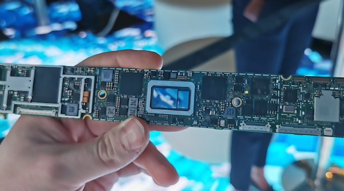
Along with detailing the nuts and the bolts of their Q1 2020 earnings, as part of Intel’s financial presentation, the company also offered a quick update on their upcoming Tiger Lake client CPUs. In short, the company is now preparing for volume production of the chips, and expects to being shipping them to OEMs mid-year.
Intel first unveiled Tiger Lake back at CES 2020 early this year, where the company briefly detailed the architecture while showing off a device using a prototype chip. Tiger Lake will be based on Intel’s latest Core CPU architecture, and will also be the first CPU from the company to integrate an iGPU based on their new Xe-LP graphics architecture. The chips will be based on a newer version of Intel’s 10nm manufacturing process than what’s used in the current ice Lake chips, which Intel is calling their 10+ process. At the time, Intel was promising that Tiger Lake devices would show up by the holidays, a similar time frame as 2019’s Ice Lake launch.
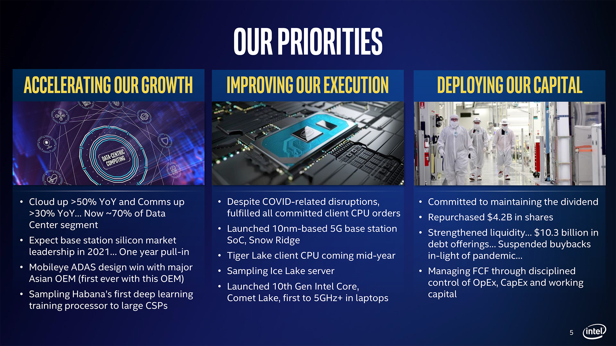
All told then, Intel’s most recent update is right in-line with their previous promises. With Tiger Lake being another mobile-first launch, OEMs need to receive chips well in advance of when consumer products will reach the store shelves, both to give OEMs the necessary time to finalize their designs, as well as to build up a suitable stockpile of devices for a proper retail launch. So, as it always needs to be said when talking about Intel’s timelines for manufacturing, while Tiger Lake chips will be shipping mid-year, we’re not currently expecting devices any sooner than what Intel has previously discussed.
Finally, if everything goes according to plan or Intel, it looks like the Tiger Lake launch should be a higher volume affair than Ice Lake’s. Cognizant of Ice Lake’s slow ramp-up and launch in 2019, Intel is telling investors that they are holding twice as many Tiger Lake CPUs in reserve as compared to Ice Lake. The company does need to master its updated 10+ process to get there, but with any luck, Intel’s 4+ years of playing with 10nm may finally pay some better dividends as they bring up their latest process.
#ontherun #TigerLake pic.twitter.com/Dhm1TwlcjV
— 𝐷𝑟. 𝐼𝑎𝑛 𝐶𝑢𝑡𝑟𝑒𝑠𝑠 (@IanCutress) January 8, 2020


140 Comments
View All Comments
Deicidium369 - Monday, May 4, 2020 - link
That is not my Reddit post. I don't post on Reddit and don't even have an acct thereDeicidium369 - Saturday, April 25, 2020 - link
what is that like the 4th or 5th iteration of TSMC "7nm"?Lakefield is Intel 10nm which is only a 2x increase on 14nm - 10nm+ (Tiger Lake) is 2.7x density.
That is TSMCs high density line - the Zen 2 CCX is less than 40M/mm^2.
see source linked below
Wilco1 - Saturday, April 25, 2020 - link
Kirin 990 5G uses the 2nd generation 7nm process, N7+ (EUV). Lakefield uses 10nm+ as Intel's slide clearly shows.Zen 2 chiplet is 52.7 MT/mm^2 using TSMC's first-gen 7nm. 14nm Xeons get just 15.8 MT/mm^2 (so about 3.3 times less dense).
We'll see how Tiger Lake does, but given it must use far more large and IO transistors than Lakefield, it'll be lucky to achieve 40 MT/mm^2, or about 2.5x scaling. Zen 3 will be out at the same time as Tiger Lake, if it uses 7nm+, density should improve to 60 MT/mm^2.
jeremyshaw - Monday, April 27, 2020 - link
To be entirely fair, the Zen2 chiplet has very little external I/O and a LOT of SRAM cache (basically best case for density), while the 14nm Xeons (assuming LGA2066 or LGA3xxx, but even the client LGA11xx/1200 somewhat applies) have a lot of I/O, much of it that has to be driven over longer distances (which drives up feature size considerably). Intel chips also come with less cache vs their AMD counterparts. So 3.3x less dense isn't exactly a straight comparison.Of course, AMD's design is made with large caches in mind, so it's not some sort of unfair comparison overall, since AMD's design uses that large cache to accommodate their slight latency penalty for having off-die I/O.
As for Tiger Lake, it has to accommodate a GPU, which are even more notoriously cache-light, lowering the density metric even further. Zen2 chiplet does not. The more interesting comparison, IMO, is Ice Lake & Tiger Lake density vs Zen2+Vega & Zen2/3+RDNA2. In these cases, AMD lowers their total cache by almost half, integrates a GPU, and also has to drive external I/O (DRAM, PCIe, USB, SATA, DP, eDP, etc). The comparison would have been less fair in the past, when the Intel U series chips had only DRAM, DP/eDP, and 4x PCIe lanes to account for (everything else was from the external chipset), but those are now joined by 4 TB3 controllers (each with 4 high speed differential pairs) basically not too dissimilar from having the SerDes for another 8 PCIe lanes, operating at a link rate between PCIe 4 and 5. Ice Lake also increases per core cache, too.
I think it's a fair comparison, as a result. Zen2 Renoir (APU) increased density to about 63.3MT/mm^2 (up from 52.7 MT/mm^2 on the Zen2 chiplet), this is inspite of decreased cache and increased I/O. Intel is treating Ice Lake-U transistor density like a trade secret, but they claim 7B transistors and measurements from Anandtech show 122.5mm^2 CPU size, giving ~57.1 MT/mm^2. Still not a straight comparison, as AMD doesn't seem to have made a low end, 7nm quad core APU this gen, and Intel only makes a quad core flagship 10nm product. Intel also still relies on a southbridge to drive the SATA, PCIe hub, USB, etc. It is within the ballpark for Intel's 10nm "high performance" variant's density claim (somewhere in the 60+ MT/mm^2 range, iirc).
Of course, this all has another problem: similar to "10nm" and "7nm" marketing names not meaning a whole lot, everyone measures "transistor count" differently, and even for the same company, the method has changed over time.
In the end, it basically means the density measurements we can get/make are almost meaningless.
Spunjji - Monday, April 27, 2020 - link
Just wanted to congratulate you on the quality of this post. Cutting through some nonsense here 👍Spunjji - Monday, April 27, 2020 - link
I'm not sure the comparison between Kirin and Lakefield is necessarily that enlightening, given how much sustained effort ARM put into optimising their designs for area efficiency on a given process technology.Renoir vs. Ice Lake ought to be a better point of comparison. Renoir runs 63.3MTr / mm^2 - I couldn't actually find numbers for ICL, though; just repetitions of Intel's original 100MTr / mm^2 claim which I believe was for NAND cells. I know it's lower than that for ICL on 10nm+, but have no idea by how much.
Wilco1 - Tuesday, April 28, 2020 - link
Lakefield is aiming to be a small low power chip like Kirin. It isn't possible to get a perfect comparison, but comparing mobile vs mobile and server vs server is quite reasonable. Either way, Renoir vs Lakefield doesn't look too good either. Despite Renoir being high-end and having more IO, it still has much better density.Bottom line - the few 10nm numbers we have show it is well behind first-gen 7nm despite all the marketing claims of 100MT/mm^2.
Spunjji - Tuesday, April 28, 2020 - link
That's a fair point - I just figure that what's effectively a first-gen product on new manufacturing tech (Foveros) is probably still not anywhere close to optimal. But you're right, that's the class of product it's effectively competing against...Definitely agreed on the last point. 100MT/mm^2 was always an aspiration at best, and anyone repeating it seriously now needs their ears rinsed out.
Everett F Sargent - Monday, May 4, 2020 - link
So, it has now been FIVE YEARS since Intel released 14mn desktop silicon (Q2'15 65W and 95W) ...https://ark.intel.com/content/www/us/en/ark/produc...
So when will Intel finally release desktop (or better, meaning at least 65W-95W parts) at any process node below 14nm? I am guessing Q2'22 or SEVEN YEARS after their 1st 14mn desktop parts.
watzupken - Monday, May 4, 2020 - link
If the first picture is the actual die size, I think it looks quite a lot bigger than the current Ice Lake U. Having used an Ice Lake U laptop, I feel that the 10nm seems to be closer to 14nm than 7nm. In fact, it seems to have regressed due to the amount of refinement over the years. Taking a quick comparison between Ice Lake and Whiskey Lake, the base clock have dropped significantly, and in some case, increased power requirement. In addition, the transition from 14nm to 10nm don't seem to help with the thermals. In my IdeaPad 5, I observed temps climbing up to 94 degs. While temp is a subjective metric highly dependent on the manufacturer's cooling solution and configuration, still 94 degs is the highest I have seen in a laptop. Even my older Ryzen 2500U don't go above 84 degs under sustained load.