SK Hynix Licenses DBI Ultra Interconnect for Next-Gen 3DS and HBM DRAM
by Anton Shilov on February 11, 2020 5:30 PM EST- Posted in
- Memory
- Nintendo 3DS
- SK Hynix
- HBM
- Interconnect
- HBM2
- HBM3
- DBI Ultra
- Invensas
- Xperi
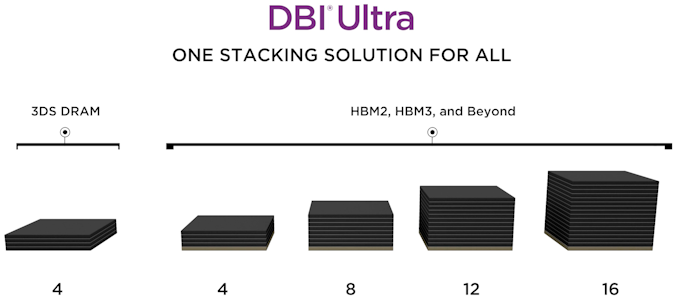
SK Hynix has inked a new broad patent and technology licensing agreement with Xperi Corp. Among other things, the company licensed the DBI Ultra 2.5D/3D interconnect technology developed by Invensas. The latter was designed to enable building up to 16-Hi chip assemblies, including next-generation memory, and highly-integrated SoCs that feature numerous homogeneous layers.
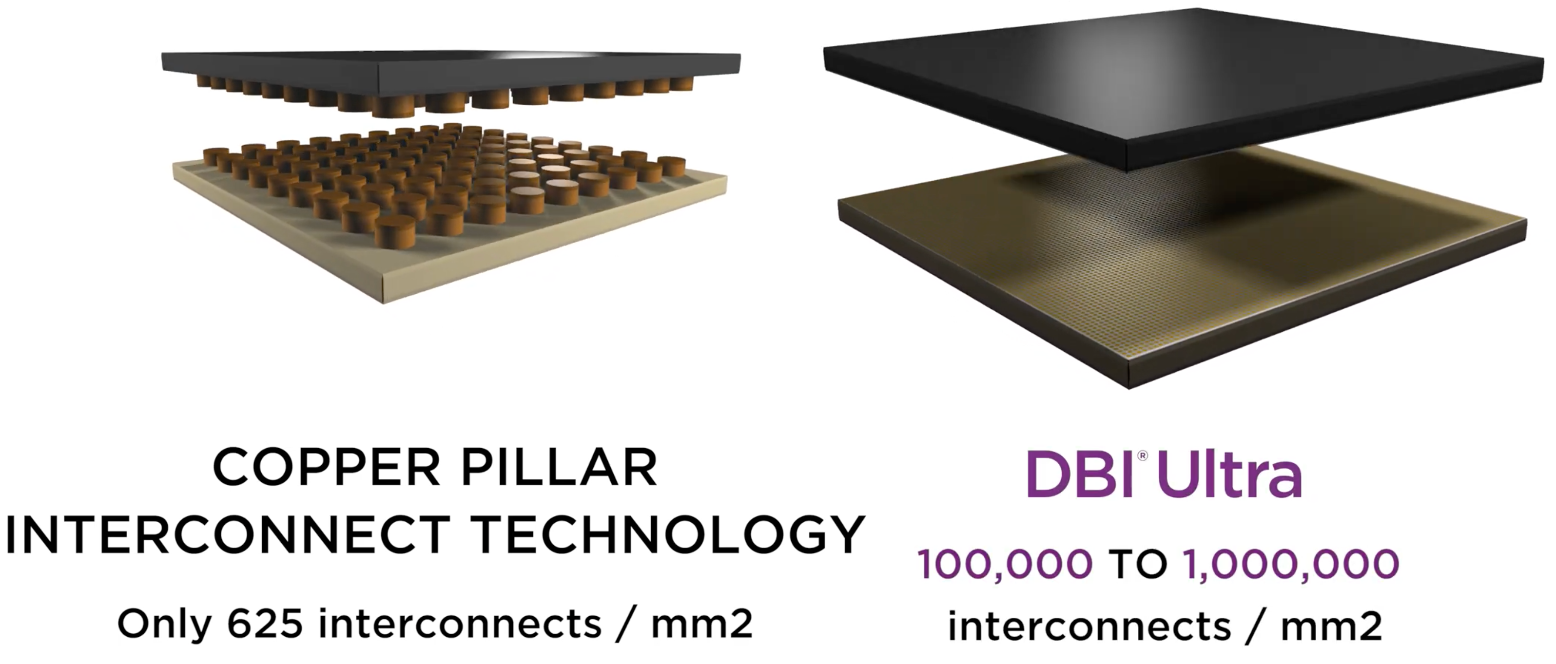
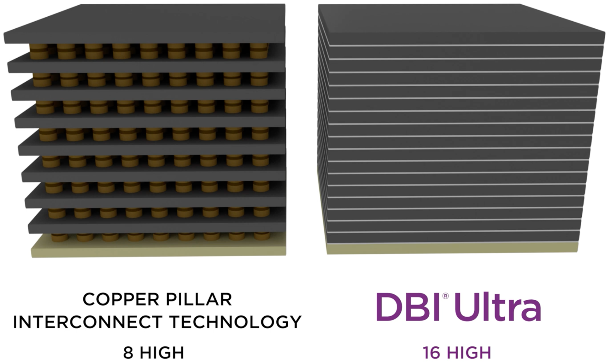
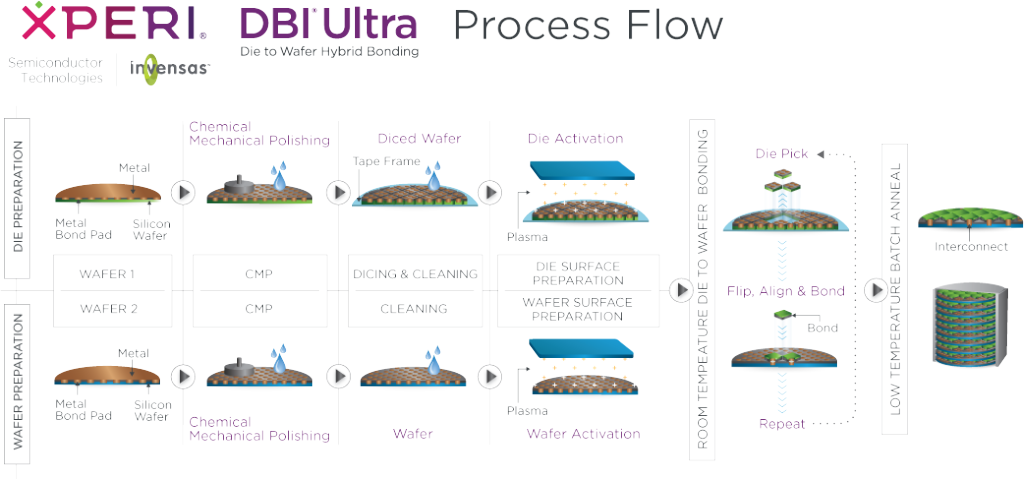
Invensas’ DBI Ultra is a proprietary die-to-wafer hybrid bonding interconnect technology that supports from 100,000 to 1,000,000 interconnects per mm2, using interconnect pitches as small as 1 µm. According to the company, the much greater number of interconnects can offer dramatically increased bandwidth vs. conventional copper pillar interconnect technology, which only goes as high as 625 interconnects per mm2. The small interconnects also offer a shorter z-height, making it possible to build a stacked chip with 16 layers in the same space as conventional 8-Hi chips, allowing for greater memory densities.
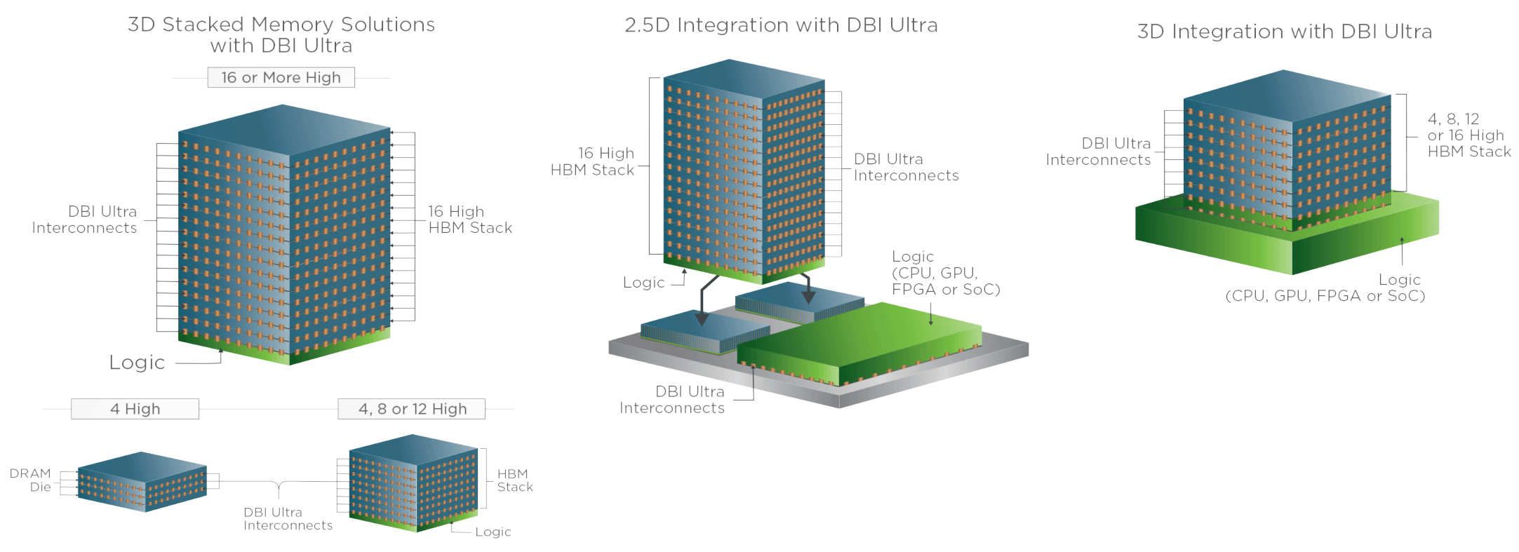
Just like other next-generation interconnect technologies, DBI Ultra supports both 2.5D and 3D integration. Furthermore, it allows integration of semiconductor devices of different sizes and produced using different process technologies. Such flexibility will be particularly useful not only for next-generation high-capacity high-bandwidth memory solutions (including 3DS, HBM, and beyond), but for various highly-integrated CPUs, GPUs, ASICs, FPGAs, and SoCs.
DBI Ultra uses a chemical bond that allows for interconnect layers that add no stand-off height, and require no copper pillars or underfill. While the process flow used for DBI Ultra is different when compared to conventional stacking processes, it continues to involve known good dies and does not require high temperatures, which results in relatively high yields.
All of this does come at a cost, however, and that's something that Invensas keeps to itself. The firm does not disclose how much DBI Ultra costs to use, or how that compares to the technologies used today.
SK Hynix does not disclose how it plans to use the DBI Ultra technology, though it is reasonable to expect the DRAM producer to use the new capability for next-generation memory products.
Craig Mitchell, president of Invensas, said the following:
“As the industry increasingly looks beyond conventional node scaling and turns toward hybrid bonding, Invensas stands as a pioneering leader that continues to deliver improved performance, power, and functionality, while also reducing the cost of semiconductors. We are proud to partner with SK hynix to further develop and commercialize our DBI Ultra technology and look forward to a wide range of memory solutions that leverage the benefits of this revolutionary technology platform.”
Related Reading:
- SK Hynix Announces 3.6 Gbps HBM2E Memory For 2020: 1.8 TB/sec For Next-Gen Accelerators
- JEDEC Updates HBM2 Memory Standard To 3.2 Gbps; Samsung's Flashbolt Memory Nears Production
- Samsung Develops 12-Layer 3D TSV DRAM: Up to 24 GB HBM2
- Samsung HBM2E ‘Flashbolt’ Memory for GPUs: 16 GB Per Stack, 3.2 Gbps
- SK Hynix: Customers Willing to Pay 2.5 Times More for HBM2 Memory
Source: Xperi


9 Comments
View All Comments