JEDEC Updates HBM2 Memory Standard To 3.2 Gbps; Samsung's Flashbolt Memory Nears Production
by Ryan Smith on February 3, 2020 8:00 PM EST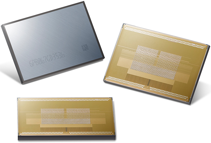
After a series of piecemeal announcements from different hardware vendors over the past year, the future of High Bandwidth Memory 2 (HBM2) is finally coming into focus. Continuing the industry’s ongoing momentum with HBM2 technology, late last month JEDEC published an updated revision of the HBM2 standard. The updated standard added support for even faster memory speeds of up to 3.2Gbps/pin, and in the process pushed the fastest speed for a complete stack of HBM2 memory to 410GB/sec. Meanwhile the memory manufacturers themselves have been preparing for this moment for a while, and Samsung has put out their own matching announcement regarding their Flashbolt HBM2 memory.
First and foremost, let’s dive into the latest version of the HBM2 standard. JESD235C, as it’s officially called, is a relatively small update to the HBM2 standard. After introducing more sizable changes a couple of years back with 12-Hi memory stacks, expanding both the speed and capacity of HBM2 memory, the latest revision is a more measured update focusing on performance.
The biggest change here is that the HBM2 standard has officially added support for two higher data rates, bringing 2.8Gbps/pin and 3.2Gbps/pin into the standard. Coming from the previous standard’s maximum rate of 2.4Gbps/pin, this represents an up-to 33% increase in memory bandwidth in the case of 3.2Gbps HBM2. Or to put this in more practical numbers, a single stack of 3.2Gbps HBM2 will deliver 410GB/sec of bandwidth, up from 307GB/sec in the last standard. Which for a modern, high-end processor supporting 4 stacks (4096-bit) of memory, this brings the aggregate bandwidth available to a whopping 1.64 TB/sec.
| HBM2 Memory Generations | |||||
| JESD235C | JESD235B | JESD235A | |||
| Max Bandwidth Per Pin | 3.2 Gb/s | 2.4 Gb/s | 2 Gb/s | ||
| Max Die Capacity | 2 GB | 2 GB | 1 GB | ||
| Max Dies Per Stack | 12 | 12 | 8 | ||
| Max Capacity Per Stack | 24 GB | 24 GB | 8 GB | ||
| Max Bandwidth Per Stack | 410 GB/s | 307.2 GB/s | 256 GB/s | ||
| Effective Bus Width (1 Stack) | 1024-bit | ||||
| Voltage | 1.2 V | 1.2 V | 1.2 V | ||
All told, this latest update keeps even a single stack of HBM2 quite competitive on the bandwidth front. For comparison’s sake, a 256-bit GDDR6 memory bus with 14Gbps memory can reach 448GB/sec of aggregate bandwidth; so a single stack of HBM2 only slightly trails that. And, of course, HBM2 can scale up to a larger number of stacks more easily than GDDR6 can scale up in bus width, keeping larger HBM2 topologies well ahead of discrete GDDR6 memory chips as far as bandwidth is concerned.
The trade-off, as always, is cost and capacity. HBM2 remains a premium memory technology – due in part to the complexities involved in TSVs and die stacking, and in part to manufacturer product segmentation – and there aren’t currently any signs that this will change. Meanwhile the latest HBM2 standard does not increase memory capacities at all – either through density or larger stacks – so the maximum size of a single stack remains 24GB, allowing a 4 stack configuration to pack up to 96GB of memory.
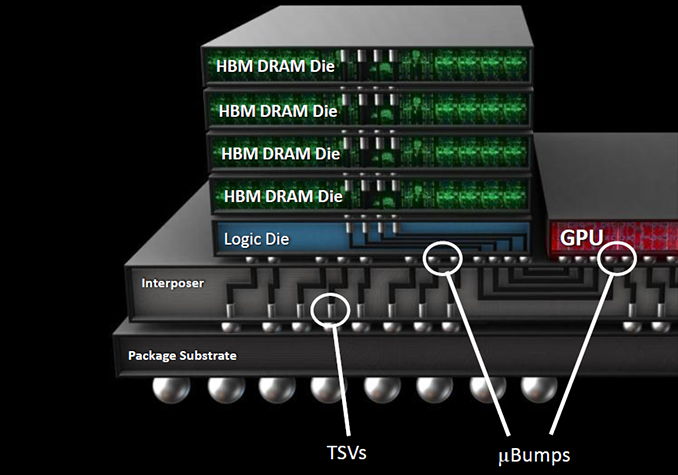
HBM In A Nutshell
Meanwhile, it’s interesting to note that as of JESD235C, JEDEC has backed off just a bit with regards to standardizing HBM2 die stack dimensions. In the previous version of the standard, the dimensions for 12-Hi stacks were listed as “TBD”, but for the new revision the group has seemingly punted on any standardization whatsoever. As a result, there isn’t a single standard height for 12-Hi stacks, leaving it up to memory manufacturers to set their own heights, and for customers to accommodate any differences between the manufacturers.
It is also worth noting that while the HBM2 standard doesn’t directly impose power limits on its own, the standard does specify regular operating voltages. HBM2 since its inception has operated at 1.2V, and the latest standard has not changed this. So the faster memory speeds should come with little (if any) increase in power consumption, as they won’t require higher voltages to drive them.
Finally, it looks like JEDEC has passed on formally adopting the “HBM2E” moniker for the latest memory standard. In pre-standard technology announcements from Samsung, SK Hynix, and others, all of these groups referred to the memory as HBM2E. And indeed, Samsung still is. However this appears to be an entirely informal arrangement, as the official wording on both the JEDEC’s page as well as in the standard itself continue to refer to the memory as HBM2. So it is almost guaranteed that we’re going to see the two terms thrown around interchangeably over the next couple of years.
Samsung Flashbolt Memory Update: Volume Production In H1’2020
Following the HBM2 standard update, Samsung this afternoon has also issued its own announcement offering an update on the status of their third-generation Flashbolt HBM2E memory. Samsung was the first company to release information on the new speeds, announcing Flashbolt almost a year ago during NVIDIA’s 2019 GPU Technology Conference. At the time Samsung’s announcement was still preliminary, and the company wasn’t saying when they would actually go into mass production. But now we finally have our answer: the first half of this year.
Given that almost a year has passed since the original Flashbolt announcement, Samsung’s announcement is as much a reminder that Flashbolt exists as it is a proper update. Still, today’s announcement offers a bit more detail than Samsung’s relatively high-level reveal last year.
| Samsung HBM2 Memory Comparison | ||||||||
| Flashbolt | Aquabolt | Flarebolt | ||||||
| Total Capacity | 16 GB | 8 GB | 8 GB | 4 GB | 8 GB | 4 GB | ||
| Bandwidth Per Pin | 3.2 Gb/s (4.2 Gb/s OC) |
2.4 Gb/s | 2 Gb/s | 2 Gb/s | 1.6 Gb/s | 1.6 Gb/s | ||
| Number of DRAM ICs per Stack | 8 | 8 | 8 | 4 | 8 | 4 | ||
| DRAM IC Process Technology | 1y | 20 nm | ||||||
| Effective Bus Width | 1024-bit | |||||||
| Voltage | 1.2 V? | 1.2 V | 1.35 V | 1.2 V | ||||
| Bandwidth per Stack | 410 GB/s (538 GB/s OC) |
307.2 GB/s | 256 GB/s | 204.8 GB/s | ||||
Of particular note, Samsung is only announcement 16GB stacks at this time, built using 2GB dies stacked in an 8-Hi configuration. And while this doesn’t preclude Samsung eventually going to 12-Hi, 24GB stacks in the future, it isn’t where the company is going to start at. The memory dies themselves are being manufactured on Samsung’s 1y process technology.
Meanwhile, Samsung appears to be setting some ambitious targets for data rates for Flashbolt. Along with supporting the new 3.2Gbps HBM2 standard, Samsung claims that they are able to go out of spec with Flashbolt, taking the memory to an even speedier 4.2Gbps. This would be a further 31% data rate increase over 3.2Gbps HBM2, and it would push the bandwidth available in a single stack to 538GB/sec, or better than half a terabyte a second. The key word here, of course, is “out of spec”; it’s not clear whether there are any HBM2 memory controllers that will be able to keep up with Samsung’s data rates, and of course there’s the question of power consumption. So while it’s all but guaranteed that Samsung has customers lined up to use Flashbolt at 3.2Gbps, it will be interesting to see whether we see any kind of high-volume products ship at data rates higher than that.
Overall, this makes Samsung the second vendor to announce out of spec HBM2 memory. Last year SK Hynix announced their own HBM2E effort, which is expected to reach 3.6Gbps. So whatever happens, it would seem we’ll now have multiple vendors shipping HBM2E memory rated to go faster than the brand-new 3.2Gbps spec.
Source: Samsung


24 Comments
View All Comments
azfacea - Wednesday, February 5, 2020 - link
not in high end GPU's with 256-384 bit GDDR6 but APU, gaming laptops are severely bandwidth limited. even ignoring price, premium gaming laptops that are TDP limited could immensly benefit from HBM but volume doesnt seem to exist for some reason.Valantar - Wednesday, February 5, 2020 - link
A bit OT first: please stop using quotation marks in that way, it makes everything you write seem intended to be ironic in a way that makes no sense whatsoever. If you say "great potential" in quotation marks like that it looks like you mean the opposite. It makes reading your posts genuinely confusing and annoying.Beyond that: HBM and HBM2 have been a significant factor in _reducing_ power draw for GPUs using it. An 8GB 256-bit high-speed GDDR5 setup - which was the main competitor in the Fiji/Vega days - uses somewhere around 40-50W. HBM/HBM2 halves that if not more. That these were relatively inefficient GPU architectures has no relation to the memory used - quite the opposite, as the more efficient memory allowed more power to go to the core, improving performance for these cards.
As for AMD card powering down when not needed - they do. Have you read a GPU review in the past ... few years? AMD has been a few watts behind Nvidia in idle power, but not much, and currently they are a few watts ahead. As for in-use voltage and clock adjustments: all modern GPUs do those too, from both vendors. AMD just happens to have a less efficient design than Nvidia (though RDNA has made major strides in efficiency they still only manage to sort of match them with a significant node advantage).
Brane2 - Monday, February 3, 2020 - link
These thgings seem like a flop to me. At leasst in their current form.They were marketed as having infinite bandwidth, compared to conventional RAM and ended up at about the same. That's a flop through a lot of orders of magnitude - it looks awkward even on logarithmic scale.
Also, all those bits have to be driven, which demands separate area for driver and connecting pad on the die. Sure, driver is smaller, but there are a lots more of them.
HBM will neded changes in underlying tech to be effective:
- DRAM cell -- that capacitor stuff is getting really old by now
- transfer signalling and protocol
If/when they solve it, HBM might be very intersting for APUs with onboard memory, extra large low latency caches etc...
A5 - Tuesday, February 4, 2020 - link
Gotta love armchair EEs. All they have to do is completely abandon the architecture? Gee, how simple!azfacea - Tuesday, February 4, 2020 - link
the combination of much higher bandwidth and lower power consumption **should** in theory make flagship smart phones very interested in HBM and much more so than AMD was for vega 56 and 64. Apple and Samsung have pretty deep pockets as well, so why arent they doing it ? what is the problem ? defect rate ??azfacea - Tuesday, February 4, 2020 - link
z-height ?? integrity/durability ??Spunjji - Wednesday, February 5, 2020 - link
Cost, plus the fact that a flagship phone would blow past its power budget doing anything that might need this much memory bandwidth.Soulkeeper - Tuesday, February 4, 2020 - link
Too bad they can't slap 2 of these on a ryzen interposer.Bandwidth per core/thread has taken a big hit over the years.
PeachNCream - Tuesday, February 4, 2020 - link
That would be nice. Giving a modern CPU one or two HBM stacks as RAM would provide sufficient bandwidth for not only the processor cores but also any iGPU needs. Integrated graphics have been held back in part by sharing bandwidth to RAM for as long as they have existed. It doesn't solve the problem of cramming all that power demand and heat into a comparably smaller space than having discrete components, but it does at least get rid of the unified memory bottleneck.FreckledTrout - Tuesday, February 4, 2020 - link
I feel like this is the end game for AMD. My guess is that we will see this around the time they move to TSMC's 3nm node. That should make for plenty of die space for 4 stacks of HBM, a 8 core CPU chiplet and a very decent GPU chiplet. Frankly I think the entire low end GPU segment for gaming will disappear around this time as well as the APU's will be good enough.