Xilinx Announces World Largest FPGA: Virtex Ultrascale+ VU19P with 9m Cells
by Dr. Ian Cutress on August 27, 2019 10:00 AM EST- Posted in
- FPGAs
- Xilinx
- Ultrascale
- VU19P
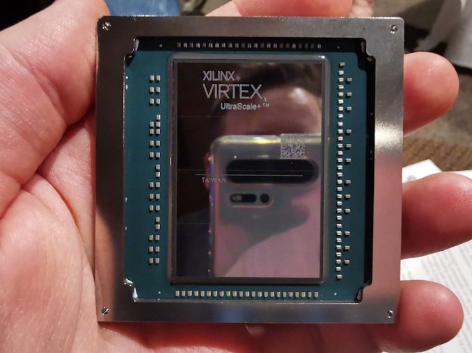
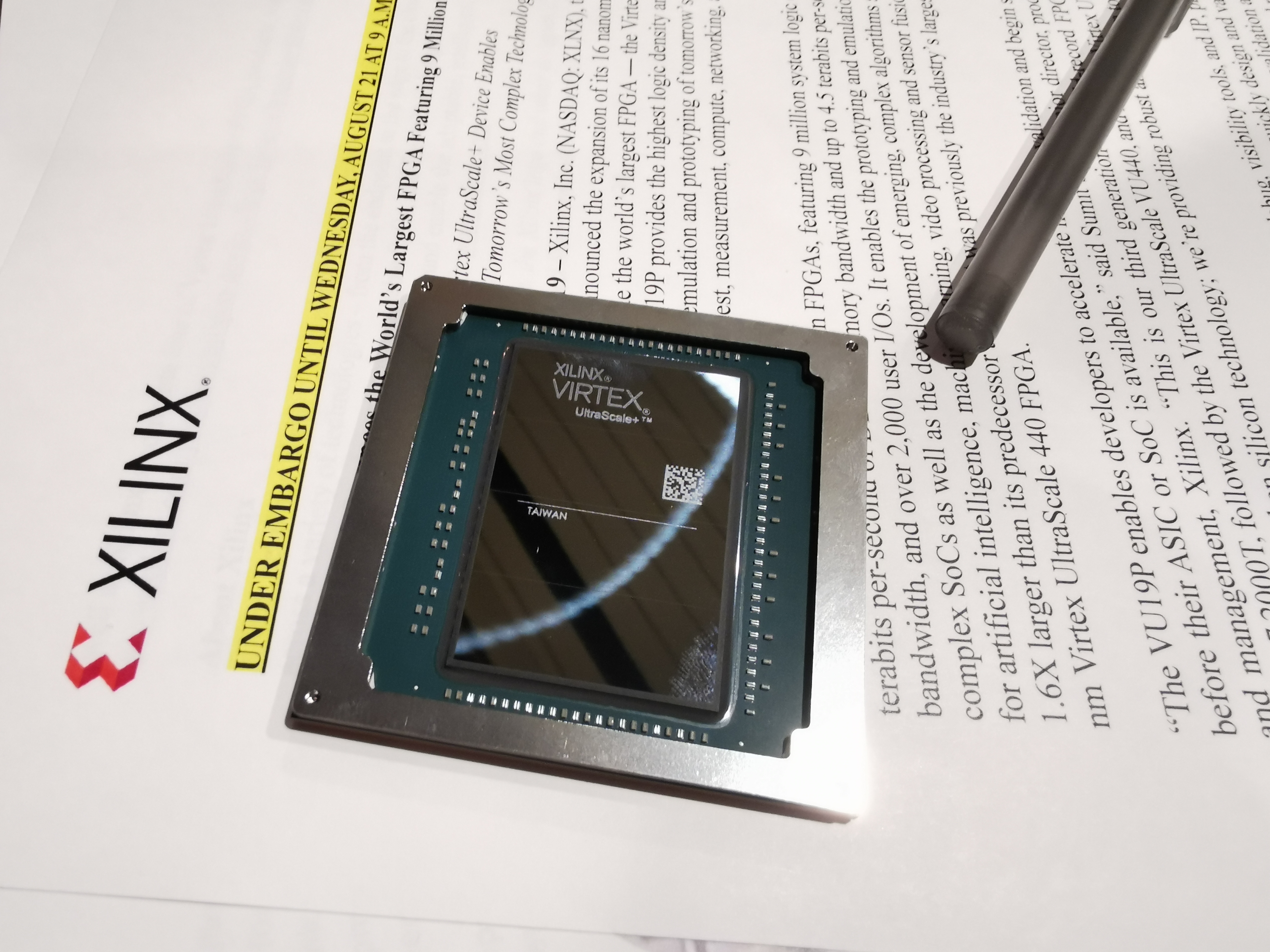
We don’t often cover the FPGA market here at AnandTech, but in the past couple of years we have seen the array of features that FPGAs are implementing expand at an incredible rate. Xilinx has been at some of the forefront of those innovations, with products such as Versal on 7nm and its Alveo family. One key part of Xilinx’s business is emulation and simulation, which requires large FPGAs to fit large designs onto - and the company recently lifted the lid on its latest creation, the Virtex Ultrascale+ VU19P. This new FPGA, when it comes to market, will hold the title of the World’s Largest FPGA.
Large FPGAs are Big Business
An FPGA, or Field Programmable Gate Array, is a bit of hardware that helps circuit designers do their job. An FPGA is so programmable that a user can design an integrated circuit on an FPGA before the design goes to market, and the engineer can see if the design works, and get rough estimates on performance and accuracy. For example, on the biggest FPGA today, Xilinx’s 22nm-based Virtex Ultrascale 440, an engineer can simulate 10 concurrent Arm Cortex A9 cores. With the new UltraScale+ VU19P, that same engineer can simulate 16 of the same cores, due to the 1.6x increase in logic gates. FPGAs also act as a base for the latest designs and technologies, with specific IO logic that can be built into current and future communication technologies. The idea of an FPGA makes it more configurable than a CPU, but that configuration can then be taken to a fab and made into an optimized chip for better performance and density. Ultimately in order to design a CPU, you need an FPGA.
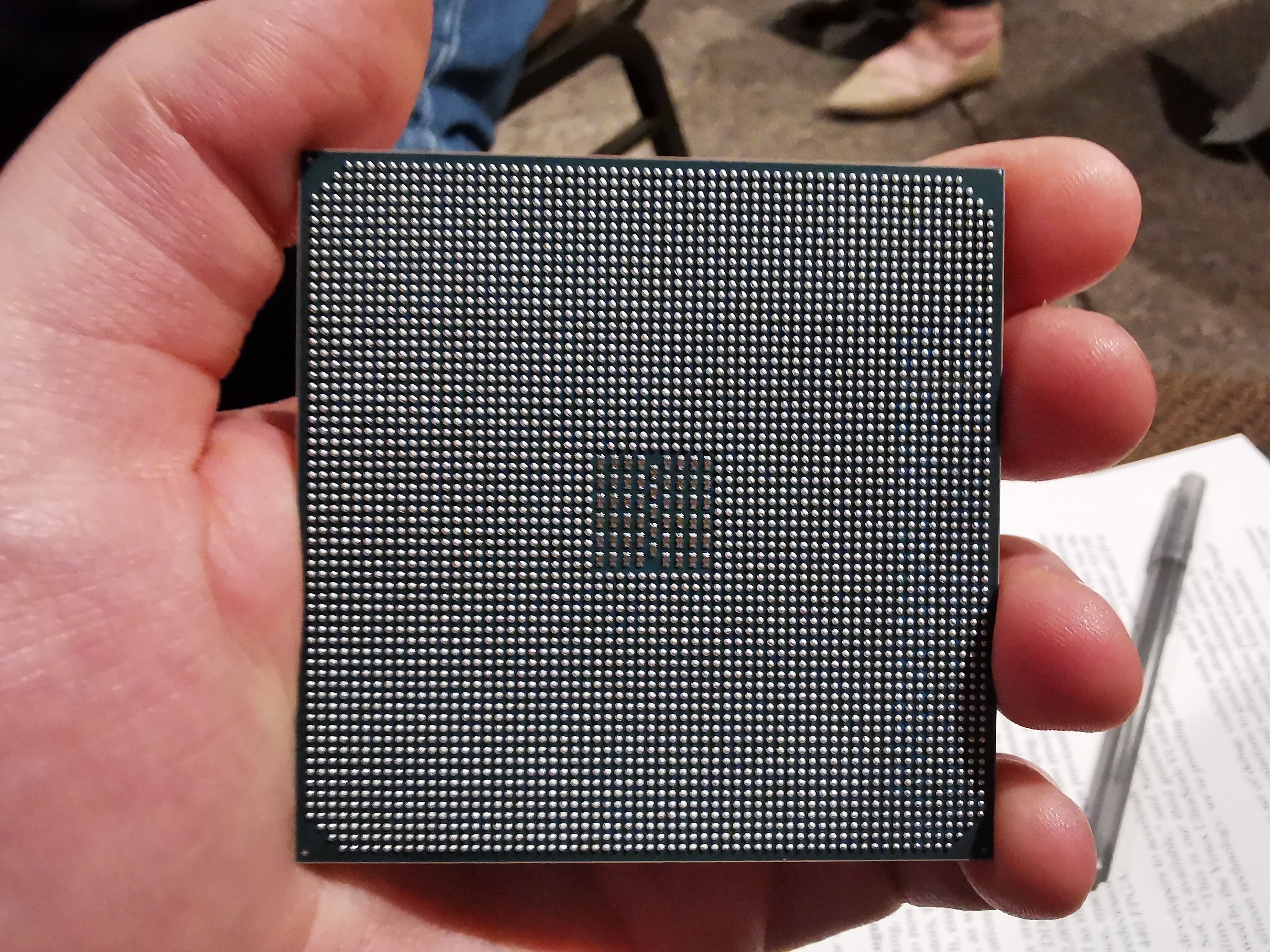
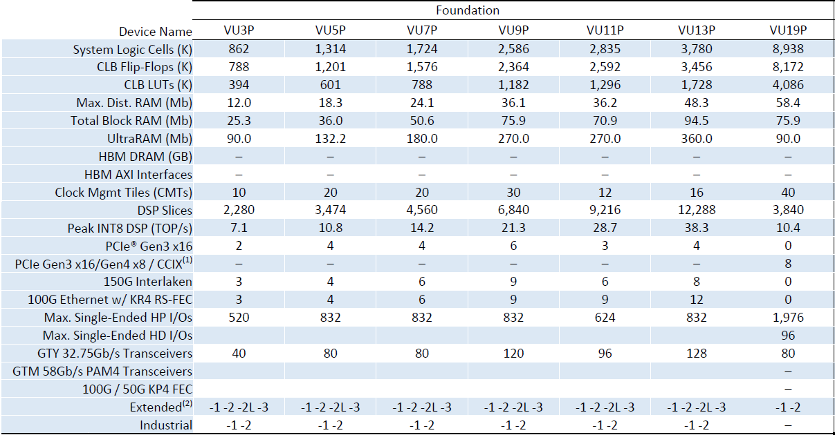
In the announcement, Xilinx explained that a sizeable part of its business is catering to this simulation and emulation market, used by all the chip vendors, and the drive to bigger chips gave them the impetus to create the VU19P. Built on TSMC’s 16FF+ process with CoWoS technology, the VU19P is actually built as four segments then placed on a die, however the chip acts as one seemless large piece of silicon, totaling 35 billion transistors. Along with the 9m logic gates, there is also over 2000 IO segments for 4.5 Terabits of transceiver bandwidth (80 lanes of 28G) and 1.5 Terabits of DDR4 memory bandwidth, which the company states will help its customers create designs featuring multiple VU19P chips in one system with all-to-all connectivity topology.
In PCIe card form the VU19P can be built as either a PCIe 3.0 x16 or PCIe 4.0 x8 device, or as a separate chip it can be used in a 65x65 package with a BGA3825 connection with the potential for CCIX connectivity. Other hardware features include 8.2m CLB Flip-Flops, 4.1m CLB LUTs, 90 Mb of UltraRAM, 40 Clock Management Tiles (CMTs), and 3840 DSP slices. Some of those numbers are quite a bit smaller than the UltraScale+ VU13P, which has only 4m logic gates, but this is due to the balancing of resources which Xilinx states will favor the simulation and emulation market.
Along with the VU19P, the company will also make enhancements to its Vivado Design Suite software to assist with co-optimization of the new chip. Xilinx is set to bring the VU19P to market in the fall of 2020 (~Q3), and will be ready to start sampling key partners in the first half of 2020.

I found a chip. It's @XilinxInc's new 'biggest FPGA ever', the Virtex Ultrascale+ VU19P with over 9 million logic cells, 35 billion transistors, and 80 x 28G IO. Built on TSMC 16FF+, coming in Q3 2020. pic.twitter.com/mn30mtenMY
— Dr. Ian Cutress (@IanCutress) August 21, 2019


17 Comments
View All Comments
SSNSeawolf - Tuesday, August 27, 2019 - link
Ian's appetite for silicon raises more questions than it answers.MrSpadge - Wednesday, August 28, 2019 - link
Well, he's still hungry for news :)asmian - Tuesday, August 27, 2019 - link
The curse of the absent editor strikes again...seamless : without seams
BurntMyBacon - Wednesday, August 28, 2019 - link
@Ian (Article): "Along with the 9m logic gates, there is also over 2000 IO segments for 4.5 Terabits of transceiver bandwidth (80 lanes of 28G) and 1.5 Terabits of DDR4 memory bandwidth, which the company states will help its customers create designs featuring multiple VU19P chips in one system with all-to-all connectivity topology."Do we not need a time scale to get a bandwidth? My understanding was that 4.5 Terabits (562.5 Gigabytes) and 1.5 Terabits (187.5 Gigabytes) are storage capacities. You would need something like 4.5 Terabits per second and 1.5 Terabits per second to get a bandwidth. Of course I could be completely off base. In which case, feel free to call me out on it and publicly revoke my data science cred.
mm0zct - Wednesday, August 28, 2019 - link
I'm pretty sure all these figures are "per second", when you're talking about a lot of bandwidth figures it's really easy to get lazy and drop the "per second" across the board.ksec - Wednesday, August 28, 2019 - link
What isn't it built on leading node like 7nm?Gondalf - Saturday, August 31, 2019 - link
Hardly you can do a such large piece of silicon on 7nm, not a way.Definition of leading node please. Advantages of a fine node: Density? true but if you can't do full reticle you are doomed. Speed? 28nm 20nm,14nm, 12nm are better. Power? modern 22nm and 20nm SOI or not SOI are better and with less power density in demanding applications. Yields? unfortunately no, they go down with geometry. Process variation? again no, crazy high right now on 10nm and 7nm. Reliablility? No. In my Knowledge only a Company can give some insurance of long term reliability on 7nm class processes.