Samsung’s Aggressive EUV Plans: 6nm Production in H2, 5nm & 4nm On Track
by Anton Shilov on July 31, 2019 12:00 PM EST
Samsung Foundry formally started to produce chips using its 7LPP (7 nm low power plus) fabrication process last October and has not slowdown development of its manufacturing technologies since then. The company is on track to start mass production using its refined 6LPP (6 nm low power plus) technology in the second half of 2019. In addition, the company said that it would tape out its first 5LPE (5 nm low power early) SoCs and would complete development of its 4LPE (4 nm low power early) process in the coming months too.
Strong Demand for Chips
Because of dropping DRAM and NAND prices, consolidated revenue of Samsung’s Semiconductor Business dropped to KRW 16.09 trillion ($14.302 billion) in the second quarter, whereas operating profit totaled KRW 3.4 trillion ($2.877 billion). While Samsung’s memory businesses were weak, the company said that its foundry business demonstrated robust results.
According to Samsung, its contract production division saw strong demand for mobile SoCs made using 10LPP/8LPP technologies as well as mobile, HPC, automotive, and network products fabbed using 14LPx/10LPP processes. Overall, it is evident that Samsung Foundry makes loads of premium products using its leading-edge FinFET process technologies.
In the next several years Samsung Foundry will continue to use its 14 nm, 10 nm, and 7 nm nodes perfected for particular applications either by optimizations or by plugging in advanced modules.
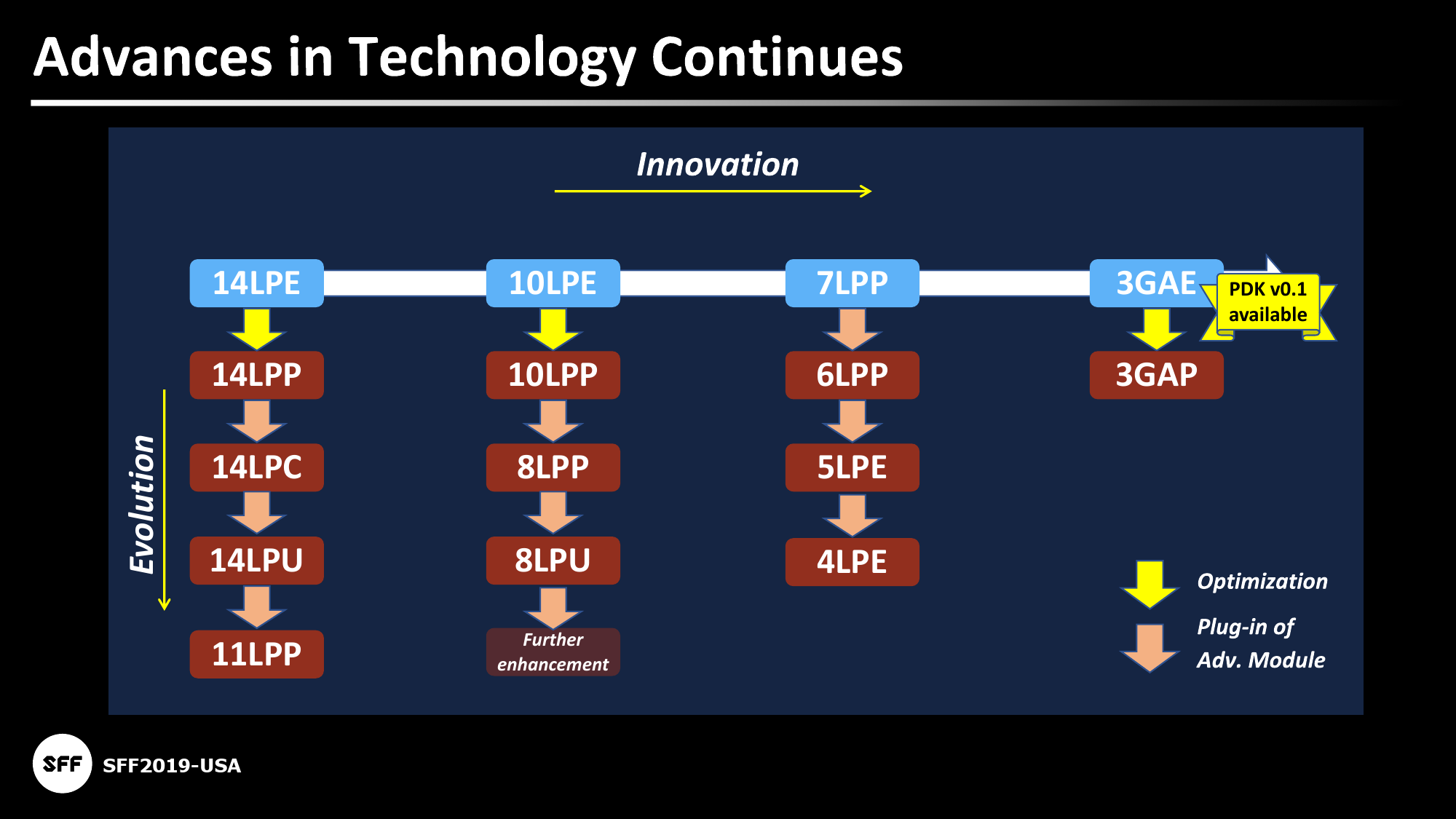
Like other contract makers of semiconductors, Samsung refines each of its nodes in order to meet requirements of various applications and clients rather than leaps ahead with radically different nodes every 18 – 24 months (like makers of chips used to do traditionally). Considering all the difficulties that engineers have to overcome developing new manufacturing technologies, the approach allows Samsung to better manage its R&D costs and manufacturing risks.
7LPP Refinements: 6LPP, 5LPE, 4LPE
As expected, extreme ultraviolet lithography (EUVL) will be a key enabler for Samsung’s leading-edge next-generation fabrication processes. The first technology to use EUV is 7LPP and its successors will use it more extensively.
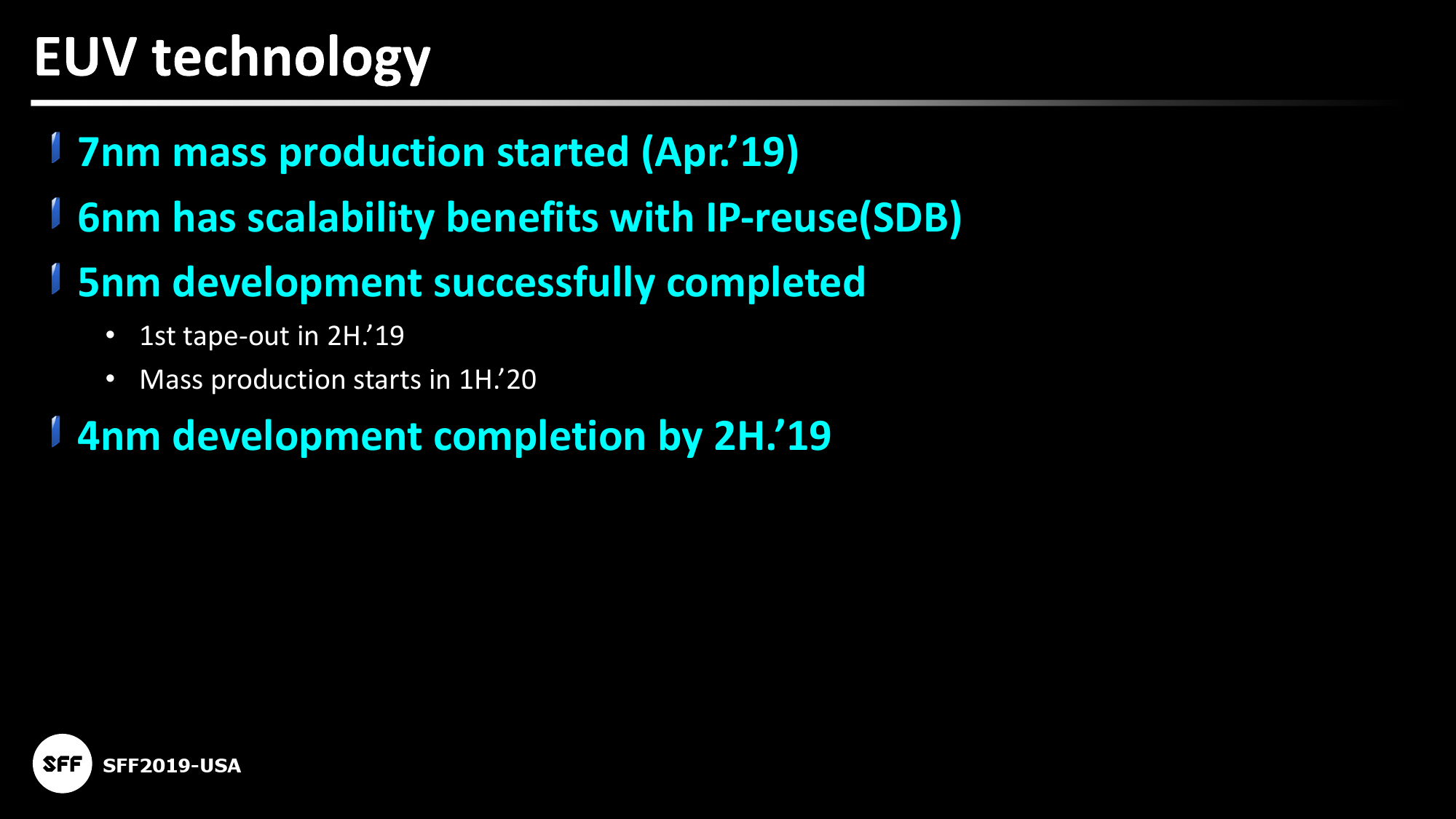
Later this year Samsung will initiate production of chips using its 6LPP process technology, which returned to its roadmap earlier. Samsung’s 6LPP is a refined version of Samsung’s 7LPP that offers higher (~10%) transistor density, lower power, but can re-use IP originally designed for 7LPP. In addition, 6LPP supports smart structures for clients willing to develop all-new new IP. As a result, Samsung Foundry’s clients will either be able to re-use their 7LPP IP without smart structures, or go with the latter, but will have to rely on new IP. In addition to smart structures, 6LPP will add support for things like multi diffusion break.
The next step in evolution of Samsung’s 7LPP production technology will be its 5LPE manufacturing process. This one provides more benefits when it comes to power, performance, and area than 6LPP, but can also reuse IP originally designed for the initial process. Samsung expects to tape out the first chips using its 5LPE technology in the second half of this year and expects to mass produce it in the first half of 2020.
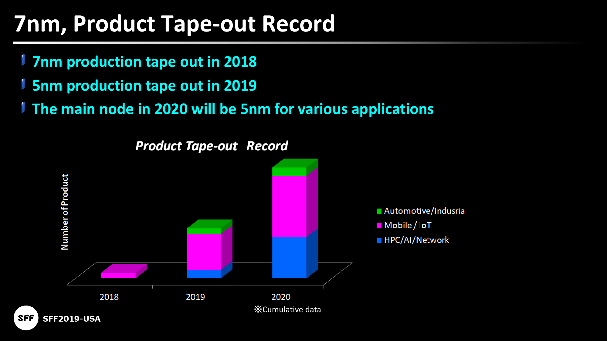
Samsung Foundry expects 5LPE to become its main EUVL node in 2020 in terms of customer tape outs, probably because the technology will be able to offer numerous benefits for a wide variety of applications, whereas Samsung’s EUV yields will get higher. Another reason why 6LPP and 5LPE technologies will be used more widely than 7LPP process is because Samsung Foundry will have more EUV capacity in the coming months after it builds its EUV line in Hwaseong, which was architected for the EUV equipment from the start. The fab, which costs $4.615 billion, will be completed shortly and is projected to start high-volume manufacturing in 2020.
The pinnacle of Samsung’s 7LPP evolution will be the company’s 4LPE technology (and possibly 4LPP that is absent from the latest Samsung Foundry roadmap). The foundry will complete its development in the second half of this year, so expect the first tape out in 2020 and volume production sometimes in 2021.
Official Statement
The official statement by Samsung about its Foundry Business reads as follows:
“For the Foundry Business, results were robust on the back of strong demand from a major customer’s 8/10-nm mobile AP and image sensor products. In addition, new orders from customers increased in the 10/14-nm process and applications diversified to include mobile, HPC, automotive and network products. In the second half, earnings growth is expected to continue due to the ongoing expansion of orders for AP, image sensors and DDI as well as increased demand for HPCs, including crypto currency mining chips. The Company plans to start mass production of EUV 6-nm process and aims to strengthen its competitiveness through tape-out of the EUV 5-nm process and by completing 4-nm process development.”
Related Reading:
- Samsung’s 5nm EUV Technology Gets Closer: Tools by Cadence & Synopsys Certified
- Synopsys to Accelerate Samsung’s 7nm Ramp with Yield Explorer Platform
- Samsung to Invest $115 Billion in Foundry & Chip Businesses by 2030
- Samsung Completes Development of 5nm EUV Process Technology
- Samsung Announces 3nm GAA MBCFET PDK, Version 0.1
- Samsung Foundry Updates: 8LPU Added, EUVL on Track for HVM in 2019
- Samsung Starts Mass Production of Chips Using Its 7nm EUV Process Tech
Source: Samsung


42 Comments
View All Comments
Yojimbo - Thursday, August 1, 2019 - link
The reticle will still be 6", it's the on-wafer field size that drops due to using a half-field in order to keep the angles of the light down. If they switched to a larger mask (9 inches) they could maintain the same maximum die size but I don't think that's what they plan to do. I guess that would be very expensive? Anyway, all that is 4 years out at least. Semiconductor companies have been researching multi-die modules for over 5 years at least, before any determinations were made on what direction high NA EUV would go, and before it was even certain that any type of EUV would be the future. There are reasons to develop multi-die modules beyond a decrease in maximum die size using high NA EUV, such as flexibility in function through modularity (more economically targeting different markets with similar IP), flexibility in using different manufacturing processes for different parts of the chip (saving on cost for less critical functions, and I believe mixing analog and digital circuitry), more power efficient pooling of compute resources for parallel processors than allowed by inter-package communication such as CLX or NVLink, and allowing scalability of architectures from something targeting an edge device to something targeting a data center through the use of chiplets.HollyDOL - Thursday, August 1, 2019 - link
No worry, average marketing guy will find a way to market "subatomic" dimensions floor tiles :-)extide - Wednesday, July 31, 2019 - link
Yes Intel's first EUV will be their "7nm" process.Santoval - Wednesday, July 31, 2019 - link
"Does it start with its 7nm?"It does, however Intel have not yet disclosed how many (and which) layers they will fab with EUV, which is just as crucial. My guess is they will employ EUV for non crucial layers. Intel's delay of EUV is not surprising. The cause is, again, their super long delay of their 10nm node. Its design was fixed many, many years ago and it predicted no EUV use (they used quad patterning instead, specifically self aligned quad patterning, for the finest details).
Intel have been fixing, debugging, optimizing, re-fixing etc their extremely complex (even for today's standards) 10nm node ever since its design was "fixed". Much more than its high transistor density (which is high in only one of its 3 variants) the reasons for the super long delay are the multiple new technologies Intel introduced at the same time, which greatly increased complexity and costs, and reduced yields. This was a strategic mistake on the part of Intel and the true reason of Brian Krzanich's departure.
Yojimbo - Thursday, August 1, 2019 - link
They will use EUV for critical layers and non EUV for everything else. Why would they use it where they don't have to? The question is how many more layers of EUV they will add beyond what is absolutely necessary, and that will depend on the productivity of the EUV tools they can achieve as well as the cost and defects they are seeing when pushing the DUV tools to do it by using multi-patterning.Santoval - Friday, October 11, 2019 - link
"Do we know Intel's EUV plan? Does it start with its 7nm?"Yes it does. They have already said they are going to use EUV lithography at 7nm but not for how many layers. Intel target at least 200 million transistors per mm^2 for their 7nm node (the 200+ MTr/mm^2 number was reported by Intel; according to SemiWiki TSMC target ~185 MTr/mm^2 at 5nm and Samsung target a mere ~125 MTr/mm^2 at 5nm, which is just ~20% denser than Intel's 10nm node).
At a transistor density of 200+ MTr/mm^2 even SAQD is insufficient, so Intel need EUV. Beyond the transistor (FEOL) stack Intel's biggest problem is with the lowest two layers (M0 & M1) of their BEOL stack. At 10nm they replaced the two lowest layers (which have the thinnest wires) with cobalt, because copper could no longer cut it due to skyrocketing resistance (which increases as the wires get thinner) and some other reasons.
These cobalt nanowires were one of the most severe issues (they contributed to the very long launch delay, the lower clocks and the lower power efficiency Intel's 10nm has than it should have had) Intel faced at 10nm, and at 7nm they would need to get *much* thinner still, which might be out of the question. Intel can still etch them with EUV with not much difficulty, but that is not the problem. The problem is that Intel will probably need to switch to another material again, with uncertain consequences.
Santoval - Friday, October 11, 2019 - link
correction : "At a transistor density of 200+ MTr/mm^2 even *SAQP* is insufficient.."trivik12 - Wednesday, July 31, 2019 - link
Samsung has not yet released single 7nm product and they have announced 3 more. More marketing bullshit. Let us see how note 7 9825(hopefully on 7nm) does before judging their plans.CiccioB - Wednesday, July 31, 2019 - link
But Nvidia that has announced Samsung as a foundry for its (probably just partially) next GPUs, which PP is going to use?I can't see a PP made for something that is not LP, and GPUs are complex and energy hungry AFAIK.
sseemaku - Wednesday, July 31, 2019 - link
They might as well call it 10 pico meter considering its a marketing name anyway without the traditional 50% scaling!