Power Stamp Alliance Exposes Ice Lake Xeon Details: LGA4189 and 8-Channel Memory
by Ian Cutress on April 9, 2018 11:42 AM EST
For everyone waiting for Cascade Lake, Intel’s next server Xeon platform, to be launched, noise is being made from the Power Stamp Alliance and its members about the platform beyond Cascade Lake. Alliance member Bel Power Solutions, along with the Power Stamp website, have exposed several details on the Ice Lake Xeon platform.
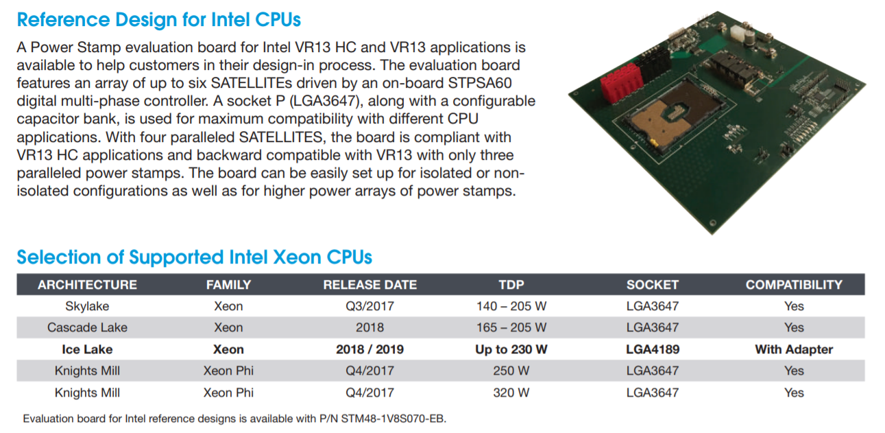
The first element of the information is the new socket, set at LGA4189. This is compared to the current Xeon socket, standing at LGA3647, which currently supports the Skylake Xeon family as well as the upcoming Cascade Lake Xeon family. According to the documents, the power pin implementation between the new LGA4189 and LGA3647 sockets are compatible via an adaptor: this isn’t to say the CPUs themselves will be, but it would appear that all the Skylake/Cascade Lake/Ice Lake Xeon families will have a similar power implementation. The reason why we mention the power implementation only is because the Power Stamp Alliance (and Bel Power Solutions) is only dealing with DC-to-DC converters for the platforms, driving efficiency from a high 48V input correlating with the Open Compute Project (OCP) standards and deployments.

Also in this image (and verified at Power Stamp) are the power ranges for Cascade Lake (165-205W, similar to Skylake Xeons) and for Ice Lake (set to go to 230W). Should the new Ice Lake Xeon platform incorporate features such as OmniPath or on-package FPGAs, which Intel has teased future Xeon platforms to be, then 230W is well within the reasons of possibility. Also, having a high DC-to-DC efficiency is going to assist with overall power consumption and power loss.
Delving into the documents, the Power Stamp Alliance designates two code names in play: VR13 (for Skylake and Cascade Lake) and VR13-HC (for Ice Lake). The HC in this case stands for high-current, and the documentation shows ‘a typical’ VR13-HC implementation with two CPUs and sixteen DDR4 memory slots for each CPU. The Bel Power systems documents goes on to say that a VR13-HC system (Ice Lake) with four power stamps meets the VR13-HC minimum requirements, while only three are needed for VR13 (Skylake/Cascade).
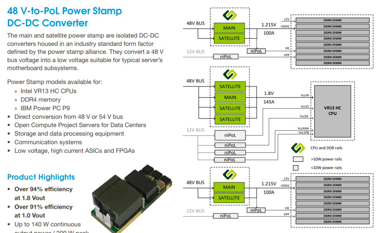
The images shown above and below point to Ice Lake Xeons being equipped with native eight-channel DDR4, given how Intel dropped 3 DIMM per channel support with Skylake. This comes through the chip directly, rather than implementing memory buffers, such as the Jordan Creek implementation on the E7 v4 family. With the 8-channel design, one might assume Intel boosting the maximum memory capacity of the base Xeon processors from 768GB to 1TB, although we should wait to see if that is going to be the case. If Intel is using the same on-chip network implementation as Skylake, it would also mean that one of the segments that previously used for a tri-memory channel controller actually has enough space for a quad-memory channel controller.
No special mention is made regarding XPoint memory support. Parts of the documents state that a set of 8 DRAM slots and two power stamps should be good for 100-200A at 1.215 V for VDDQ, implying that a set of 8 memory sticks should be able to draw around 120W-240W, or ~15-30W each. Varying numbers have been postulated as to the power draw of XPoint modules, but most numbers are within this range.
More information from the Power Stamp Alliance is set to be given at the Open Compute Summit, happening in late May. The Alliance consists of STMicroelectronics, Artesyn Embedded Technologies, Bel Power Solutions, and Flex
Sources: Bel Power Solutions, Power Stamp Alliance, via Twitter
*This article first stated that the OCP Summit was going to happen in Late May. It actually happened in Late March already.


37 Comments
View All Comments
close - Tuesday, April 10, 2018 - link
Innovation is so hard and expensive... when the competition isn't on your heels.But here's some not so veiled "let's defend Intel because that's why we're here" argument: "The argument from Intel was that only 5% of the market needed that amount of memory per socket". What you're not saying is that it was followed up by "and since those 5% have few alternatives we're going to squeeze them dry".
The market doesn't have much choice in the matter so Intel can milk it. It's not like you'll just quickly switch to AMD based servers.
A couple of years ago Ian Cutress was promoting and supporting Intel's argument that the market doesn't need more than 4 cores and that building such a CPU is prohibitively expensive and too technologically challenging to build which is why they're targeting just the ultra-enthusiast. Ryzen launched shortly after. And lo and behold, Intel found another 2-4 cores in their pocket to tack on to the old CPUs with barely a price change. They also found that the market wanted and/or needed more cores. And whaddayaknow, they even make a profit on them.
But don't let Intel's history of constantly lying about their overcharging and lack of solid progress YoY get in the way of defending them. I'm sure this time it's fo' real.
iwod - Tuesday, April 10, 2018 - link
I dont think there is only 5% of market needing that at all, it is simply because Memory has becomes ridiculously expensive. So few years ago we were hoping the $1000 DRAM would drop to $500, instead it is now $2000.Kevin G - Monday, April 9, 2018 - link
Cascade Lake is due with Optane DIMM support. I fathom the M suffix will be the only SKUs that will support them due to their expected capacity advantage over LR-DIMMs.iter - Tuesday, April 10, 2018 - link
Oh goodie, can't wait for overpriced memory modules that cr@p out in week of typical usage.There are things I would use hypetane for, but under tight scrutiny in terms of usage patterns. Shoehorning it into a ram socket and role is tremendously stupid, because performance is piss poor compared to dram, and endurance is practically pathetic. If you don't keep a tight control over the usage, it will wear out in zero time.
Which is good for intel anyway, since they still struggle hard to sell poor hypetane.
lurker22 - Monday, April 9, 2018 - link
Can't include 1 line in the entire article that defines what the heck is the power stamp alliance?vgray35@hotmail.com - Tuesday, April 10, 2018 - link
Its a collusion of forces engineered to maximize profitability of the power chip manufacturers at best, but it seems the acumen of its members leaves a lot to be desired, and hence are likely to damage the industry given enough time to be allowed to prevail in their agenda.Kevin G - Monday, April 9, 2018 - link
" If Intel is using the same on-chip network implementation as Skylake, it would also mean that one of the segments that previously used for a tri-memory channel controller actually has enough space for a quad-memory channel controller."Alternative take 1: Intel is increasing the core size so there is now room for two quad channel memory controllers on-die.
Alternative take 2: Intel decreased the die size and is now using four dual channel memory controllers on-die.
It is bit too early to tell which one is reality.
Ian Cutress - Monday, April 9, 2018 - link
^^ thisHStewart - Monday, April 9, 2018 - link
To me this looks like they are moving to EMIB technology on Xeon chips - probably on other lines also. This could mean multiple CPU or CPU and GPU.Also adapter sounds like a way to make motherboards handle older processors - or possibly mean
new motherboards will be upgradable to new processors.
One thing interesting is that Power Alliance page does not include Intel as member. when it looks aim at Intel products.
Kevin G - Monday, April 9, 2018 - link
EMIB seems to be a natural way to scale up core counts and additional logic on package. I would expect that the memory controllers and IO get spun off into their own separate dies as that would simply matching the requisite IO for each socket: 2066, BGA 2518 (Xeon D), 3647, 4189 etc.