Change of Strategy: A New GlobalFoundries CEO in Dr. Thomas Caulfield
by Anton Shilov on March 15, 2018 1:00 PM EST- Posted in
- Semiconductors
- GlobalFoundries
- IBM
- 7nm
- FD-SOI
- 5nm
- 12FDX
- 22FDX
GlobalFoundries 2014-2018: Key Goals
Sanjay Jha was hired as CEO of GlobalFoundries in early 2014. While management changes are never explicitly explained, and in case of the privately-held GlobalFoundries are not discussed in depth, his key goals as the head of GF were more or less obvious.
- Firstly, Mr. Jha had to ensure timely development and deployment of leading-edge process technologies.
- Secondly, the CEO had to increase production yields across all nodes and fabs at GlobalFoundries to ensure that the company is competitive and has strategic relationships with its partners (who would not need to second-source their ICs from TSMC, UMC or SMIC).
- Thirdly, he had to expand GF’s products offerings to ensure the company’s abilities to address different types of customers and land new clients.
- Fourthly, he needed to expand production capacities of GlobalFoundries to sustain relevancy of the foundry to existing customers and open up doors for new parties particularly from the mobile and IoT spaces.
- Last but not least, he had to create a culture of sustainable development of new technologies and profitable growth for the company. Creating a company that can consistently deliver on its promises is hard, it will take years to realize whether Mr. Jha has succeeded, but the GF BOD appears to think so.
Hitting strategic goals involved achieving tactical objectives, and while Mr. Jha has managed to do a lot, there was one thing that he has failed: to make GlobalFoundries profitable. Given the expansionist strategy, this was barely possible. But while expanding product lineup and boosting capacities, GlobalFoundries managed to increase its sales by over 40% from 2014 to 2016 (more on that later).
GlobalFoundries Process Technologies
Our avid readers remember GlobalFoundries’ origin, being from AMD’s manufacturing arm. Historically, AMD would only need one competitive manufacturing technology for its high-performance CPUs and could slightly alter it for mobile parts. The production organization within AMD was tailored to develop one advanced fabrication process at a time while also maintaining one fab in Dresden, Germany. When at some point Hector Ruiz (CEO of AMD from 2002 to 2008) decided to build another fab in the upstate New York, USA, he thought of offering other companies access to its production facility and process technology, but not becoming a fully-fledged foundry. AMD never planned (at least publicly) to offer a dedicated production process for non-CPU applications, such as GPUs (which need high transistor densities rather than maximum clocks), even after it acquired ATI Technologies in 2006.
Due to financial difficulties, AMD had to spin-off their manufacturing operations into a new company in March 2009. Then, GlobalFoundries’ parent company ATIC acquired Chartered Semiconductor in September to add manufacturing capacities and technologies for mainstream chips and make the new company more competitive overall. While GlobalFoundries became the No. 2 contract maker of semiconductors overnight, its leading-edge team remained the same as if the operations were a part of AMD: one fab, one process tech. GlobalFoundries struggled with 32 nm/28 nm HKMG technology in 2011 – 2012 and their roadmap did not look strong later on. Enter, Sanjay Jha.
When Sanjay Jha joined GlobalFoundries, the company had a major problem. Its 20 nm-based 14XM (14 nm eXtreme Mobile) fabrication process has failed to gain traction among developers of mobile SoC as was barely suitable for the company’s key customer, AMD. In a bid to get things right quickly, GlobalFoundries had to ink a deal with Samsung Foundry and license its 14LPE and 14LPP manufacturing technologies. The two contract makers of semiconductors said in their mutual press release that they would be able to jointly land orders from major customers and therefore compete for large clients against TSMC. This part of the plan has not really worked out (at least publicly GlobalFoundries has never admitted it had produced chips for customers it landed together with Samsung), but GlobalFoundries obtained a competitive fabrication process that later enabled it to make CPUs and GPUs. Moreover, further development of the 14LPP (called the 14HP) is used to make IBM’s z14 CPUs for mainframes.
Since GlobalFoundries has struggled to develop competitive leading-edge manufacturing technologies, the next challenge for Sanjay Jha was to make sure that his company would be able to develop competitive processes going forward, for which it needed some additional talent. In a surprising move, GlobalFoundries acquired IBM’s microelectronics business unit along with fabs, personnel and customers. Under the terms of the deal, IBM paid GF around $1.5 billion in cash to take the business, and gave GF access to its leading edge manufacturing patents, but in exchange GF was obliged to serve IBM’s clients and to produce IBM CPUs made using custom fabrication processes for the following 10 years (until 2024). Development of custom manufacturing technologies will eventually cost billions of dollars, but IBM can pay a lot for its CPUs and hopefully GlobalFoundries at least will not lose money on these projects. In any case, taking over IBM’s microelectronics business unit was the only way to obtain talent along with various RF and SiGe process technologies, so Mr. Jha had to take the risk.
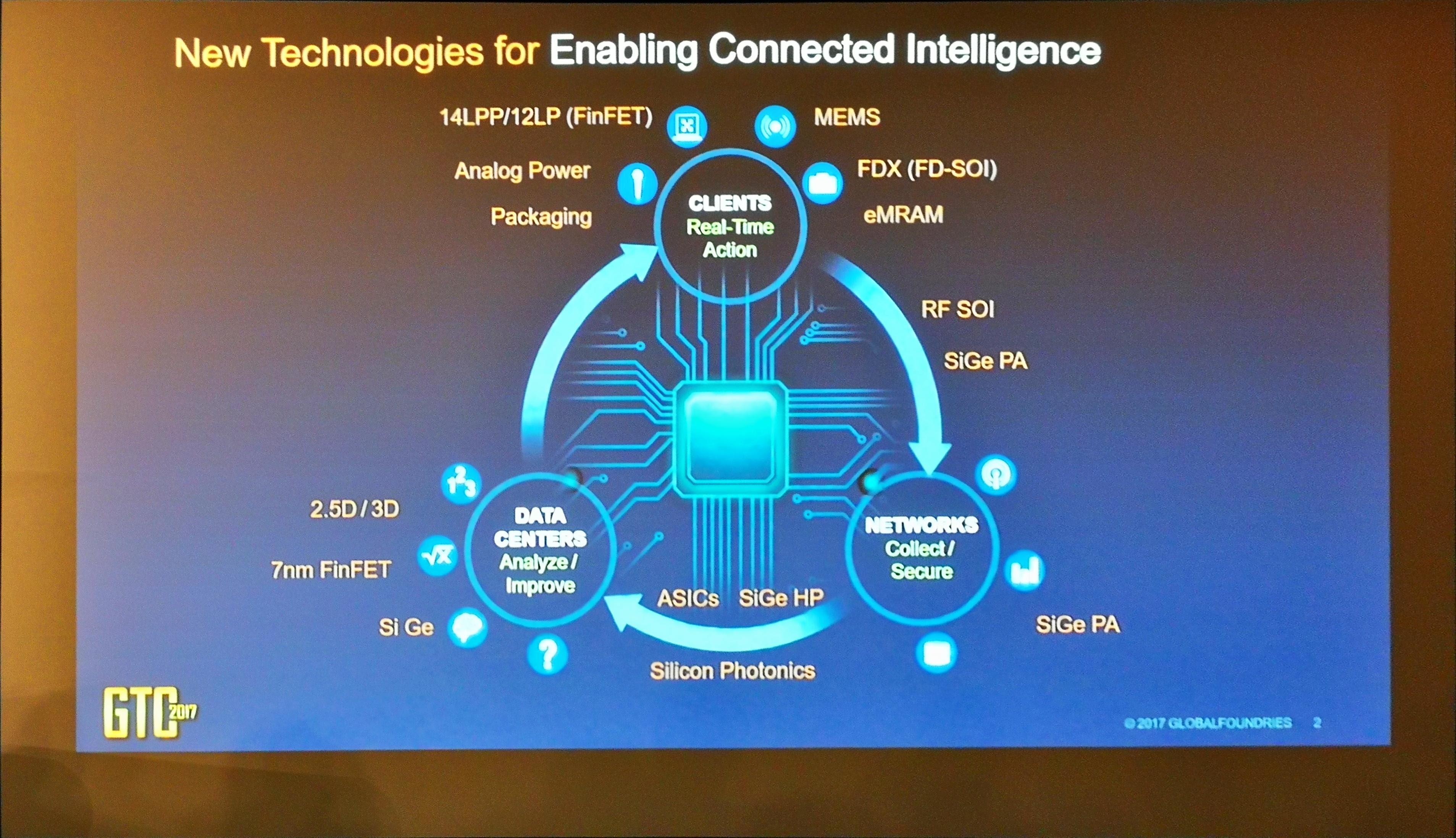
Procuring unique RF, RF-SOI, and SiGe technologies from IBM brought a set of crucial competencies to GlobalFoundries and greatly expanded its lineup of offerings to clients. In fact, radio technologies defined GlobalFoundries’ focus and corporate motto going forward: Enabling Connected Intelligence. Selling mainstream application processors and RF solutions for such chips seems like a good business in the upcoming 5G era. Keeping in mind that GlobalFoundries can also produce CPUs for datacenters and various silicon photonics interconnection solutions, it is clear that the company can address virtually all types of today’s and tomorrow’s applications (from a smartwatch all the way to a datacenter with PCs and smartphones in between).
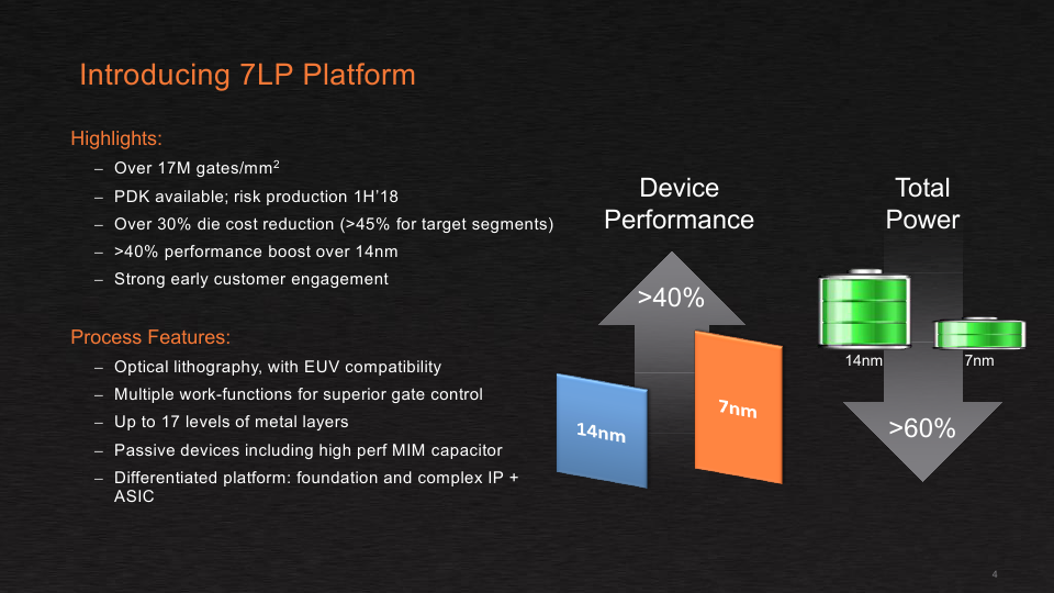
Obviously, GlobalFoundries stumbled very badly at 14 nm (so it had to license it from a rival), but instead of trying to catch-up with other contract makers of chips ASAP by bypassing a '10nm node'. The company decided to leap forward to a 7 nm-branded process tech developed by the joint team of IBM and GlobalFoundries engineers (essentially burying 10 nm technologies started by both companies). General specifications of GF’s first variant of the 7LP process technology uses deep ultraviolet (DUV) argon fluoride (ArF) excimer lasers with 193 nm wavelength. These processes are relatively well known, but we also know that the company plans to offer three generations of the technology, two of which will use EUV lithography. Something less known is that there will be five different versions of GF’s 7 nm node aimed at different applications.
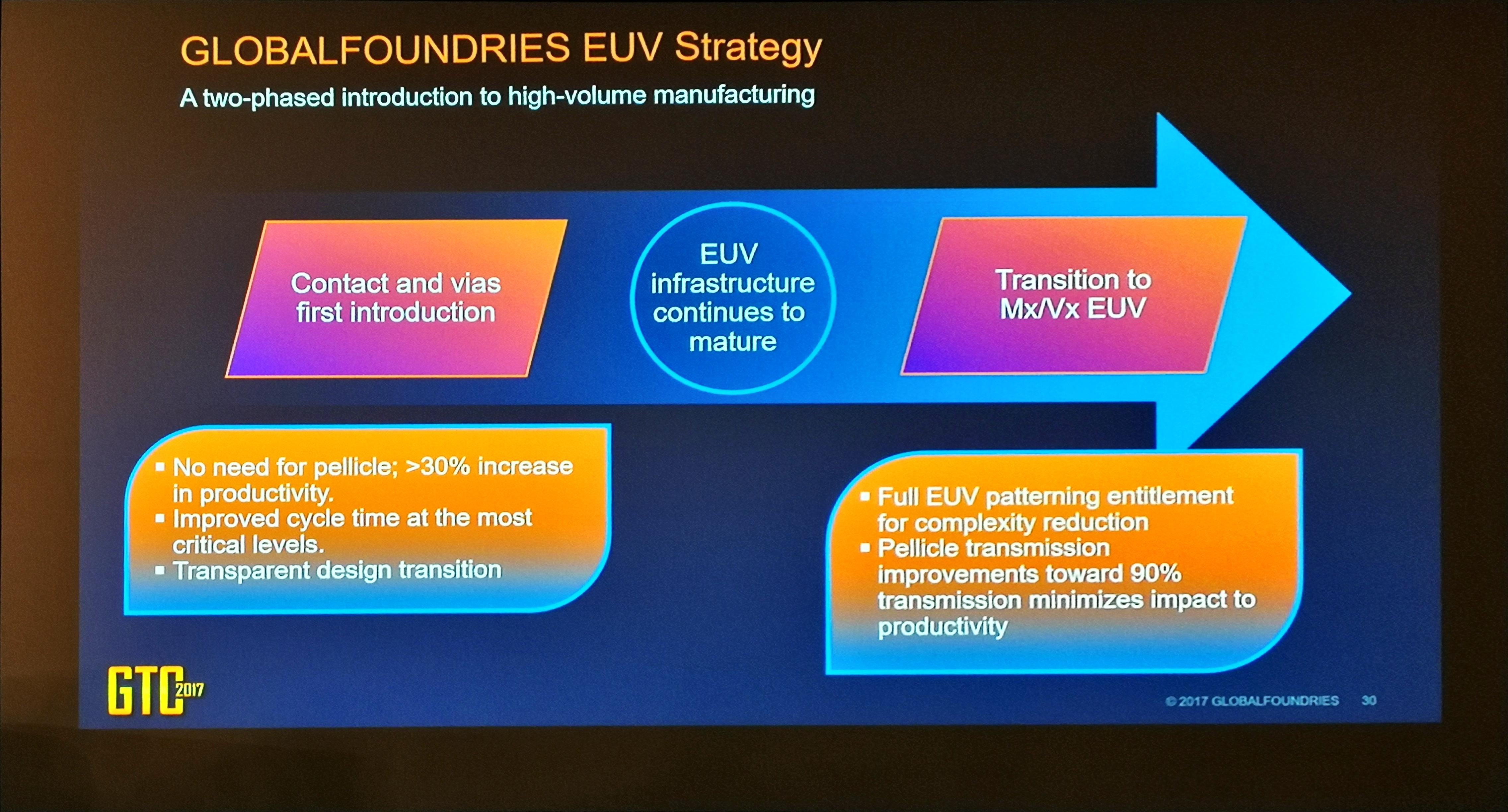
When it comes to EUV progress at GlobalFoundries, last year the company announced intentions to install two ASML TWINSCAN NXE step and scan machines into the Fab 8 in 2H 2017. As of February ‘18, only one of such tools have been installed, with another waiting to be built, but keeping in mind that the company only plans to start using its EUV equipment commercially in 2019, a slight slip in the schedule is not going to cause any problems.
Having obtained talent for further development of leading-edge process technologies and IBM’s RF/SiGe business, GlobalFoundries' management team remembered about customers who cannot afford development of chips featuring FinFETs or more advanced transistor structure (going FinFET can triple development costs, and not all companies can invest $80 - $90 million in a mainstream SoC).
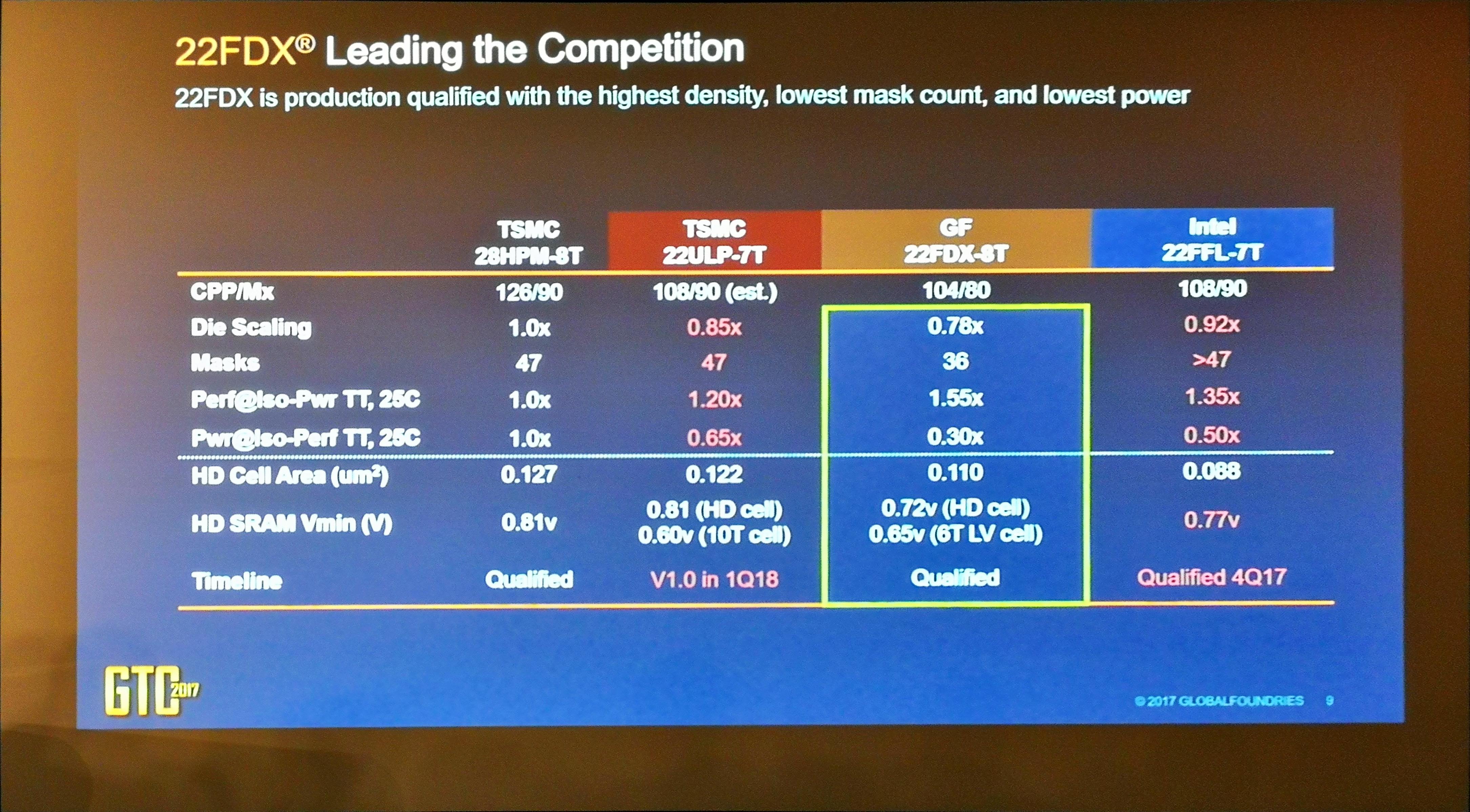
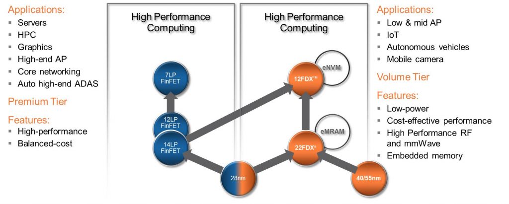
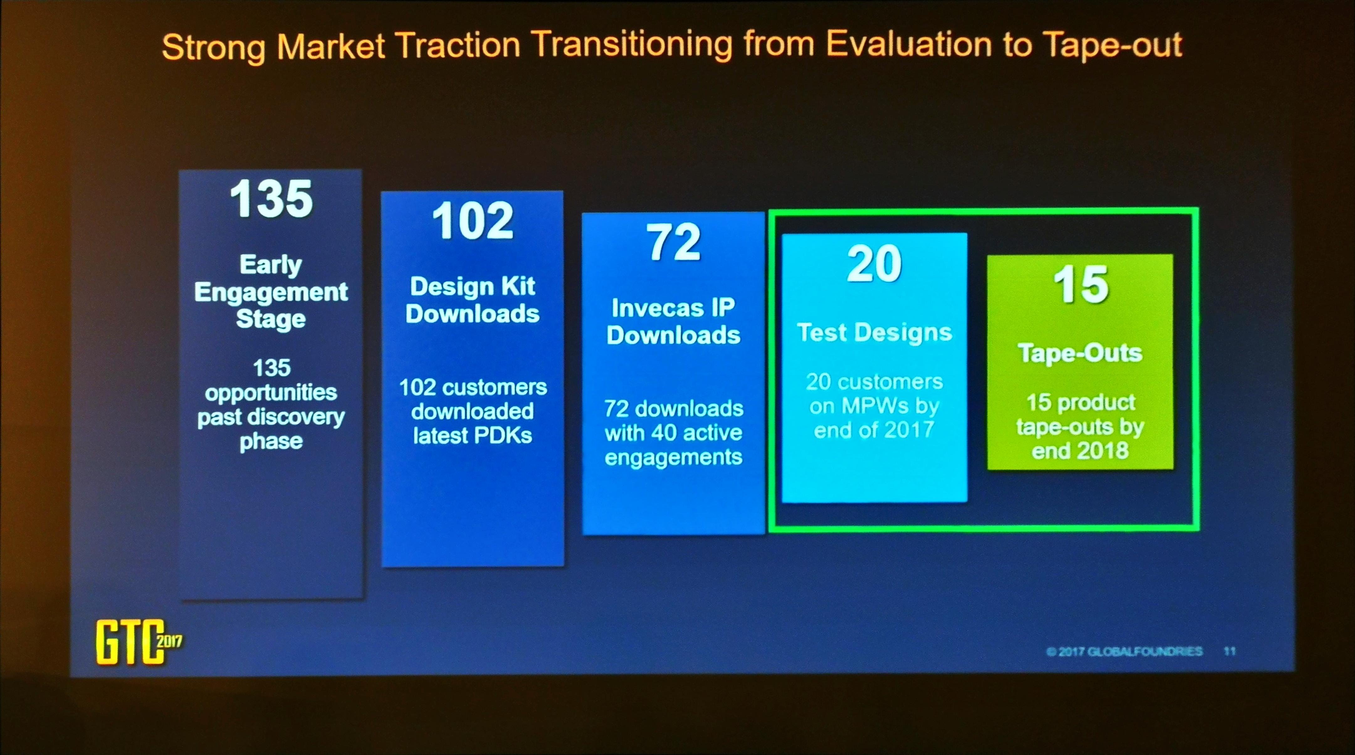
A right fabrication process for such clients would be an enhanced technology with planar transistors, which is why GlobalFoundries adopted FD-SOI for its 22FDX manufacturing process in mid-2015. The 22FDX uses back-end-of-line interconnect flow of STMicroelectronics’ 28nm FD-SOI, the front-end of line of STM’s 14nm FD-SOI process technology, and planar transistors. Based on GF’s data, the 22FDX looks very competitive against other sub-28 nm low-power fabrication processes and it has been qualified for production for about a year now. The interest towards the 22FDX is strong: 15 tape-outs are expected by end of 2018 (and for what it is what it’s worth, it is more than TSMC has seen with its CLN10FF, even though the two technologies are incomparable).
In late 2016 the company extended its FD-SOI roadmap to the 12FDX manufacturing tech, targeting applications that need higher complexity and/or performance. The 12FDX promises to offer a 26% performance improvement or a 47% lower power when compared to 22FDX, which brings it close to 10-nm-class process technologies from competing companies. Considering the fact that FD-SOI-based process technologies promise to enable lower IC development costs (because of planar transistors), the 12FDX promises to be a success, assuming that GlobalFoundries can produce it with decent yields and at high volumes.

Keep in mind that advanced FD-SOI-based manufacturing processes are only offered by GlobalFoundries and Samsung Foundry, so from a certain point of view GF’s FDX effort resembles a blue ocean strategy.
Before we move on to manufacturing capacities, let us put GlobalFoundries’ ongoing strategies related to process technologies into perspective. The contract maker of chips has two development paths for ICs: leading-edge 7nm/5nm nodes featuring FinFETs/GAAFETs, and FD-SOI-based nodes featuring traditional planar transistors. Strategically, it means that even if GF struggles with the leading-edge, it will still have tens (if not hundreds) of logic customers with advanced FD-SOI ICs. In addition, GlobalFoundries has a variety of RF technologies that will gain importance going forward.
When Sanjay Jha joined GlobalFoundries in early 2014, the company only had one leading-edge process technology on its hands, 14XM, and only a few customers were interested in it. Now, GlobalFoundries will have at least five leading-edge promising fabrication processes for the coming years: 12LP (an enhanced 14LPP), two/three generations of 7 nm, and two generations of FD-SOI-based offerings (22FDX, 12FDX).


14 Comments
View All Comments
ZolaIII - Thursday, March 15, 2018 - link
Well not a really interesting article...How about writing more about 14HP FinFET-SOI & beyond.
III-V - Thursday, March 15, 2018 - link
Ah yes, FDSOI... the transistor vaporware. Real interesting stuff, there...ZolaIII - Thursday, March 15, 2018 - link
I told 14HP which is 14nm FinFET structure on SOI wafer and beyond 14nm... FD-SOI is hire to stay & badly needed for G5, mimo x4 in mobile, IoT and cetera basically all RF blocks & CMOS on it is coming too.BestGuess - Thursday, March 15, 2018 - link
The article states that 14HP is a descendant of 14LP from Samsung, but more likely it is a marriage of IBM's internally developed 14nm SOI process and 14LP. See IBM's last publication on it prior to the acquisition:http://ieeexplore.ieee.org/abstract/document/70469...
The descriptions of IBM's Power9 chips, which indicate it is SOI and features embedded DRAM, sure look a lot more like the IBM technology than the bulk 14LP technology...
As for RFCMOS applications, FDSOI could be a game changer, since as a planar technology, it doesn't suffer from the high gate capacitance of Finfets. This capacitance is part of the Finfet advantage for Logic applications, but is a real handicap for RF, which requires dealing with much higher frequencies.
ZolaIII - Thursday, March 15, 2018 - link
Yes I reed that article long time ago so do I really need to quote my self again? 14HP FinFET-SOI and beyond.GF 22 nm FD-SOI isn't game changer but a winning design & for digital it's proven how it can match the best efforts on 10 nm FinFET regarding power consumption when back biasing is used that is 0.4V (for small to medium sized SoC's) while analogue where it's obviously only logical choice goes with 0.8V. For most things & especially IoT you need to use combined multi RF & digital components in the same package & that it's both development and final product price is cheap so it's absolute design win for both RF and IoT and good enough for mainstream, it's also win for DSP's not so much for FPGA's & GPU's as they tend to be huge but in smaller or mobile ones it still wins because of its price. Only thing where it loses is HPC & desktop CPU which tend to push operating frequencies as much as possible & FinFET is better at this...
Cooe - Thursday, March 15, 2018 - link
I'm happy with this choice. IBM produces great tech executives. Just look at Lisa Su.TheJian - Saturday, March 17, 2018 - link
You must be kidding. They should have kept Dirk Meyer who said in 2011, we need to make a KING product in cpu/gpu FIRST, then do this APU/console crap that has junk margins that are merely additive, rather than the bulk of your net income. You can use junk like that to milk your tech for the last few dollars but like NV/Intel, AMD should be concentrating on the enterprise stuff or rich people PERIOD. After that leaves cards or chips on the shelf, THEN and ONLY then do you chase the low margin products.If you are limited in supply (can't produce them as fast as you sell them I mean), which is the case for both AMD/NV currently, you shouldn't be wasting time on 10-20% margins (which for AMD just means barely break even on a good quarter), but rather you should be chasing 50%+ margins.
For anyone who doesn't believe this is how things work (they fired Dirk for saying it...LOL, morons), you should just compare the last decade of NV & Intel quarterly reports to AMD's. Note Intel plops chips on TOP of their stack when adding new models (HEDT anyone?), and NV simply put out 1080/1070 (for example) and took a year to put out a 1060. No point in wasting silicon on poor people (sorry, just the facts) when you can nab a RICH person who has throw away cash sitting all around him and upgrades yearly :) At anything under 30% margins AMD just ends up barely paying interest on their debt, wafer agreement penalties etc. They need to hit 40%+ before they start rolling in cash. They should have hit servers first, then home users. IE, I'd rather be chasing $1000-7000 cpus if I was AMD instead of chasing <$1000. They just put out an APU that has a max price currently of $169...ROFLMAO. Lisa should be fired (and most of their management, they are clueless), and Dirk should be sought out ASAP. He was right. Well, DUH.
Now worse IMO, they are giving Intel IP, instead of MAKING THAT CHIP THEMSELVES! Intel will probably charge $400+ for the 8809g. That should have been AMD. AMD is probably making peanuts on that, while Intel takes the bulk of the profits. If I was AMD's CEO I'd fire anyone who brought me an idea that didn't make 40%+ margins out of the gate at least. Intel/NV are chasing 60% stuff and higher. They'd be 70% margins overall if they axed the bottom...LOL.
Not a knock on IBM people, just on this person. Letting Intel/NV have the high end for basically most of the last 7yrs, is retarded. Consoles killed R&D that should have kept them in the cpu race, and drop watts/heat on products, allowed proper R&D to not have crap launches with problem after problem (mboards not having bios' finished, memory issues, vid cards launching and having to speed up fans to mitigate issues etc). With anyone but a fanboy, you probably only get ONE chance to impress your customers. You can't screw up a launch if you're the little guy, you need to get that right out of the gate. Who's idea was it to launch a month or two early damaging the cpu launch? Not the Motherboard makers...AMD had ~800mil to survive one more month (one more year easily), so why push the launch too early? You're fired. Who chose SINGLE DIGIT console margins for 2yrs (they finally said mid double digits-meaing 15% or less or you'd say 16+ right?), instead of CPU/GPU/DRIVERS R&D? You're fired too. Who chose HBM not once, but TWICE, when it was worth nothing more than a buzzword as that bandwidth was not needed at all (see NV cards). It still isn't needed now either which is why all NV home cards have GDDR5x or less, and why their margins are GREAT and setting record profits/margins/revenue quarter after quarter. Who decide a buzzword was worth the risk of massive shortages and super high BOM costs which kills margins (and card supply). If you can't get it on a shelf, your tech is useless. NV chose the KISS principle. For AMD management, who'm I'm sure hasn't heard of this (LOL), it stands for KEEP IT SIMPLE STUPID. AMD went hard to produce, wasteful (overkill bandwidth when only unicorns were using 4K...LOL) and expensive. NV chose easy to make, cheap, and adequate for even Titan. Again AMD management, do you read quarterly reports (your own, and your competition?)?? No? You're fired. Come back when you understand basic economics. Price wars as the only broke guy in the room?? LOL. I digress.
zodiacfml - Saturday, March 17, 2018 - link
If it was that easy, they did just what you said, with pleasure.However, AMD's technical ability can't keep up with Intel and Nvidia. Therefore, it has always been AMD's last resort to choose better memory for performance gain to keep up. This is the reason why AMD has been first with integrated memory controllers, HBM, and choosing higher bandwidth memory spec for some cards vs. competing cards of Nvidia
They're pretty lucky with this as the cryptocurrency ethash/Ethereum algorithm is memory intensive, making their cards superior for mining despite behind in gaming performance or other crypto algorithms. It should have been a quick fix for their profitability by producing more cards but they are limited by the shortage of memory.
Thermalzeal - Friday, April 6, 2018 - link
AMD Can't keep up? That is the most interesting thing that causes my eyebrow to raise, that has been said in a long time :P It's a full stack of technical implementation and AMD has led the market in pushing the tech forward while Intel has bunny suits and disparate architectures for rich people.I honestly can't stand Intel Fanboys, sure if you actually flex your computational power in a single socket you can drain your capex like a cray (see what I did there) but truly if you want to zen out and achieve more sustainable opex AMD has been a leader.
Intel has only achieved it's success with 25x pockets. So, I really don't think any respect is due to Intel Engineers for marketshare that is complete hogwash. AMD has always done more with less, and unfortunately had complete useless humans like Hector Ruinz destroy the company and Global Foundries.
Galcobar - Thursday, March 15, 2018 - link
"Sanjay Jha, who lead the world’s..."Led.
Past tense of the verb lead is led. Not that English makes it easy since the pronunciation for the noun lead is the same as the past tense verb led.