Samsung Launches Z-SSD SZ985: Up To 800GB Of Z-NAND
by Billy Tallis on January 29, 2018 9:00 PM EST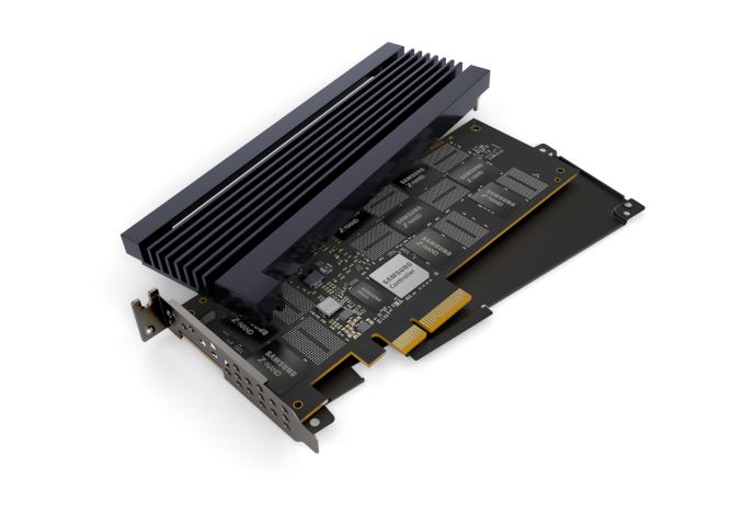
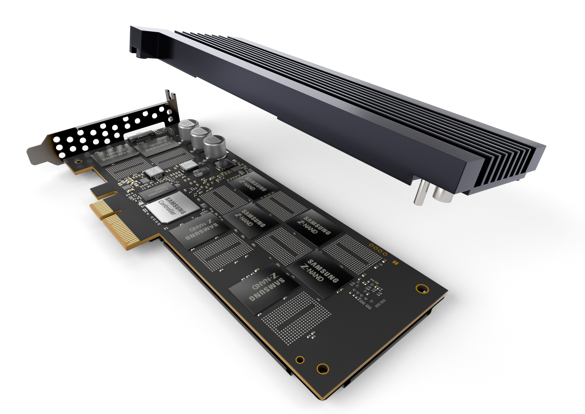
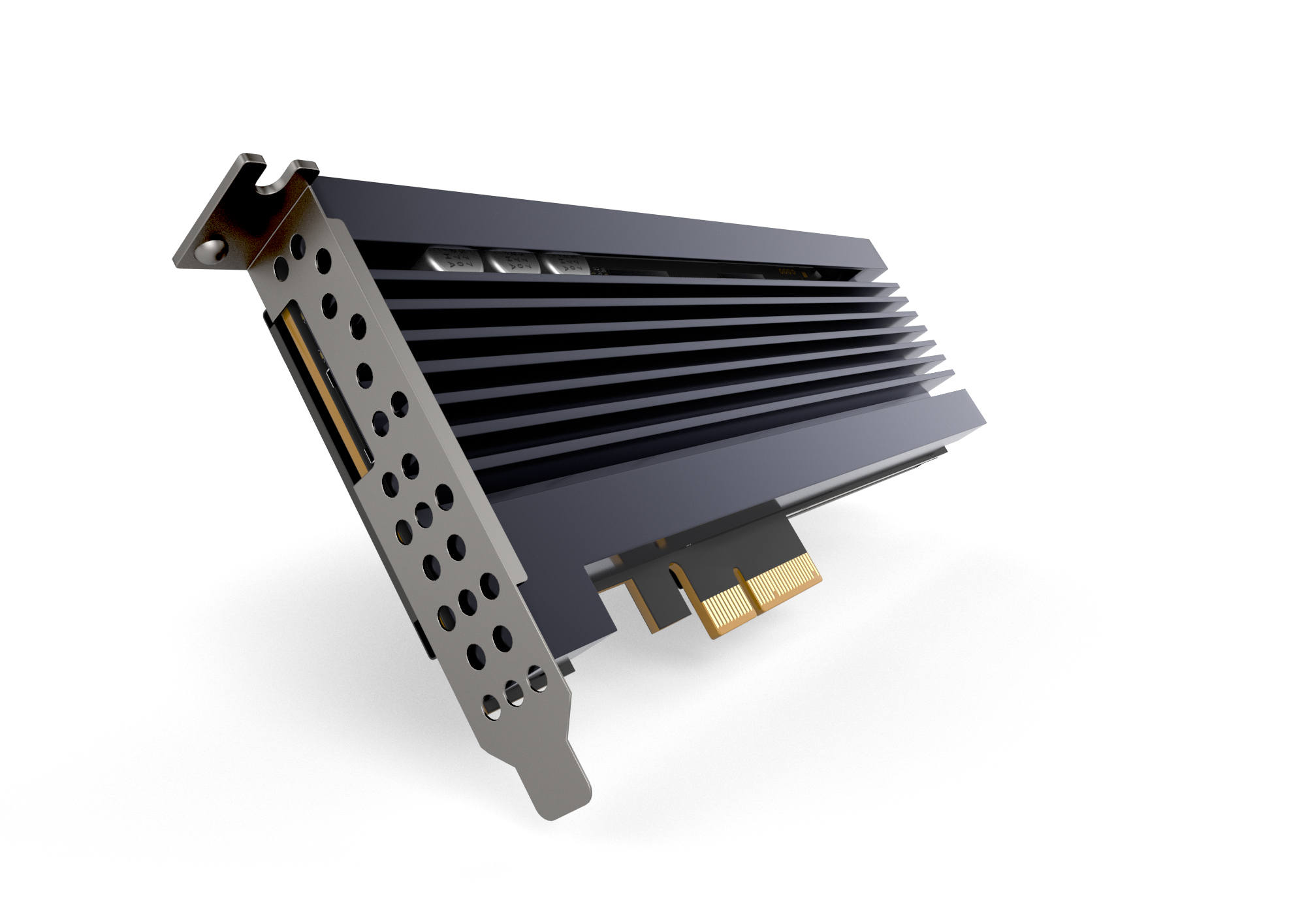
Samsung announced today that they are officially launching their first Z-SSD product, the SZ985. The Z-SSD uses Samsung's Z-NAND memory, a high-performance derivative of their 3D NAND flash memory and Samsung's intended competition for Intel's 3D XPoint memory. The SZ985 is a high-performance, high-endurance enterprise NVMe SSD.
Samsung has been talking about Z-NAND and the SZ985 for quite a while, including showing off prototypes at several trade shows and conferences. Their initial announcement in 2016 of Z-NAND memory and Z-SSD drives promised 1TB drives in 2016 to be followed by 2TB and 4TB drives in 2017. Today's launch of 800GB and 240GB models is far behind that initial timeline, but the Z-SSD is finally ready for broad release, almost a year after Intel's Optane products first hit the shelves. Samsung hasn't provided much new information about how the Z-SSD works under the hood, but they have disclosed that the drive includes 1.5GB of LPDDR4 DRAM. This suggests that the Z-SSD either has huge overprovisioning with as much as 1.5TB or Z-NAND memory for the 800GB model, or that the Z-NAND is being managed in a way that requires more than the usual 1GB of DRAM per TB of NAND flash used by most SSDs.
Samsung has not provided full performance specifications for the SZ985, but they have highlighted several key metrics that put the Z-SSD in the top performance tier. The SZ985 can deliver up to 750k random read IOPS, well above the 550k IOPS that Intel's Optane SSD DC P4800X is rated for. Write performance from the SZ985 is much less impressive at only 170k random write IOPS. The random write speed rating on Intel's P4800X is only 9% slower than the random read speed, while the Samsung SZ985 will have a random write speed that is 77% slower than random reads. Samsung has not been able to overcome all of the limitations of flash memory, but they have produced some impressive improvements.
Samsung also makes a few comparisons against more mainstream enterprise SSDs based on 3D TLC NAND flash memory. The memory cell read performance of their Z-NAND is ten times higher than their 3D TLC NAND, leading to 70% higher random read throughput than their PM963 NVMe SSD. Exact read latency isn't specified, but write latency on the SZ985 is quoted as 16 µs.
Despite not having record-setting write performance, the SZ985 is still designed to handle very write-intensive workloads. The endurance rating is 30 drive writes per day for five years, matching Intel's Optane SSD. However, both drives still fall short of the long-gone Micron P320h SLC NAND SSD, in both performance and endurance (though Intel has at least exceeded the random write speed of the P320h). Samsung's most significant accomplishment with the Z-SSS SZ985 is likely that they can offer the performance of planar SLC at much lower cost thanks to their 3D NAND structure.
Samsung will be presenting the Z-SSD SZ985 at the International Solid-State Circuits Conference, February 11-15.
At Flash Memory Summit last year, Samsung announced a second generation of Z-NAND memory. The SZ985 is still a first-generation product, and drives with the second-generation Z-NAND could still be a long way from launching.
Source: Samsung


45 Comments
View All Comments
iter - Tuesday, January 30, 2018 - link
I guess that CPU cache is just "sone of the dram used as sram", right?PeachNCream - Tuesday, January 30, 2018 - link
At least one SSD manufacturer states they simulate SLC functionality using a portion of the TLC capacity. It appears that XabanakFanatik's statement is accurate.https://support.ocz.com/customer/en/portal/article...
iter - Tuesday, January 30, 2018 - link
If that is the case, where is the benefit of launching znand as a "mlc used in slc mode" when:1 - it doesn't seem to offer any capacity benefit - 800 gb is quite modest for mlc, we've seen 2tb in a tiny m2 drive already
2 - it doesn't seem to offer any performance benefit - it is barely faster than mlc, and the advantage can be attributed to a better controller, it is nowhere nearly as fast as slc.
As for toshiba's "explanation" - it is either a technically inaccurate layman's version of what is going on, or a bad case of cutting corners, because even though technically it is possible to save some time writing only one bit, the writing process is still significantly slower than slc due to the cell design. Current drives that employ slc caching certainly behave like they have a discrete and static amount of cache rather than using some portion of the available main memory.
PeachNCream - Tuesday, January 30, 2018 - link
I can't speak for Samsung when it comes to justification regarding the release of Z-NAND so I won't address your concerns about it or about whether or not the performance justifies a new product release.As for SLC caching, the amount of TLC assigned as cache is static. A portion of non-resizing TLC is dedicated to SLC operating mode which explains why you can reliably replicate benchmark results to demonstrate a point in time when performance declines as write activity is forced outside the SLC mode space. The information in the link I provided is accurate though. There is no special SLC only memory in a modern TLC drive.
Lolimaster - Tuesday, January 30, 2018 - link
CPU cache is actual low latency/high performance/costly memory totally different from dram, that's why they're used on KB sizes for L1 and a few MB's for L2-L3.EDRAM is a bit slower than L3 but still much faster than typical DRAM which is why the Broadwell chips with GT4e gpu's using the built in 128MB of EDRAM as "L4 cache" were performing miles ahead of any other cpu at certain tasks like file compression&encrypting (like 5-10x).
Flunk - Tuesday, January 30, 2018 - link
No, DRAM and SRAM are totally different. "SLC Cache" as the device makers call it is when they store only one bit per MLC or TLC cell for better performance. It's a pretty standard industry practice.chrnochime - Wednesday, January 31, 2018 - link
Who's the one who needs to be educated here anyway LOLtuxRoller - Tuesday, January 30, 2018 - link
Since the manufacturers absolutely can (and do) operate their mlc cells in SLC mode (called pseudoSLC, but the reason why is a bit subtle and maybe not too meaningful) then HD sorts be looking to be cautious of Vespa!From everything I've read there seem to only be a few differences between SLC and the others. Those differences are: size (SLC is usually built using larger, 2X or higher, process nodes which allows for larger voltage differences), and only needs to differentiate between two states. Moving an M/TLC cell to SLC means you get as large of a voltage difference between states as if the cell had been made SLC, at the same process, from the start. There's some complications that I'm ignoring (mostly involving the more sophisticated error correction/detection mechanisms, the idea of partial writes with the corresponding need to be able to detect the smaller voltage differences of each state and write dis) but this is what I'd expect Samsung to have here (the degree to which they've changed the internal and external controllers is the real unknown here).
Lolimaster - Tuesday, January 30, 2018 - link
No, you don't get it. Don't fall for snake oil tactics.SunnyNW - Tuesday, January 30, 2018 - link
Billy is there a way to test how many voltage levels there are per cell?